High-Bay Industrial LED MCPCB
Tailored for high-wattage stadium, mining, and warehouse flood illumination where extended 50,000+ hour lifespans under continuous 70°C ambient temperatures are non-negotiable.
An authoritative technical analysis of Metal Core PCBs (MCPCB): resolving junction temperature bottlenecks, evaluating ceramic dielectric formulations (1.0 to 5.0 W/m·K), mitigating mechanical shear stress in LED packaging, and managing global high-volume OEM supply chains.
Why solid metal substrates outperform conventional FR4 in photonics: breaking down the physics of thermal transfer across multi-layer MCPCB stacks.
High-power solid-state lighting systems convert approximately 30% to 40% of input electrical power into visible photons, while the remaining 60% to 70% dissipates directly as localized waste thermal energy. In high-density LED arrays—such as automotive matrix headlamps, horticultural grow bars, stadium floodlights, and industrial high-bay fixtures—failing to conduct this thermal flux away from the semiconductor P-N junction causes severe catastrophic degradation. Junction temperatures (Tj) exceeding 85°C to 105°C accelerate phosphor degradation, induce massive chromaticity shift (color drift), reduce luminous efficacy (lumens per watt), and trigger premature bonding wire fatigue.
An Aluminum Core LED PCB Board (also referred to as an Aluminum-base MCPCB or IMS - Insulated Metal Substrate) delivers an efficient conduction path that is 5 to 10 times more thermally conductive than traditional epoxy-glass FR4 substrates. A precision-engineered single-layer aluminum board consists of three interlocked metallurgical and chemical layers:
| Layer Element | Standard Thickness | Material Chemistry & Function | Key Performance Metric |
|---|---|---|---|
| Circuit Foil Layer | 1.0 oz to 4.0 oz (35µm – 140µm) | Electrolytic or rolled copper etched to create circuit traces and LED component mounting pads. | Carries forward operating current up to 30A with minimal resistive I²R heating. |
| Thermally Conductive Dielectric | 75µm to 150µm (0.075 – 0.15 mm) | Specialized epoxy-resin matrix densely compounded with micro-ceramic particles (AlN, Al₂O₃, or Boron Nitride). | Thermal conductivity: 1.0 – 5.0 W/m·K; AC Breakdown voltage: >3.0 kV to 6.0 kV. |
| Aluminum Base Core | 0.8 mm to 3.0 mm (standard 1.6 mm) | Industrial-grade aluminum alloys, predominantly AL-5052 (high tensile strength) or AL-6061 (machinable/flat). | Thermal conductivity: 138 – 180 W/m·K; acts as structural backplane and primary heat spreader. |
| Reflective White Solder Mask | 20µm to 35µm | Titanium dioxide (TiO₂) enriched polymer formulated for zero UV yellowing and high diffuse reflectance. | Luminous optical reflectivity: 88% to 92% diffuse bounce; heat resistance to 260°C reflow. |
In standard FR4 laminates, through-plane thermal conductivity sits at a negligible 0.25 to 0.3 W/m·K. While thermal vias with copper plating can mitigate localized hot spots, the high thermal impedance of fiberglass woven cores creates an unsustainable thermal barrier. In contrast, an Aluminum Core LED PCB utilizing a high-efficiency 3.0 W/m·K dielectric slashes the overall thermal resistance down to less than 0.8°C/W.
By conducting thermal energy directly downward through the dielectric and into the aluminum alloy substrate, heat is distributed laterally across the metal plate and efficiently coupled into secondary extruded aluminum heatsinks or active chassis enclosures. This thermal equilibrium protects delicate driver ICs, electrolytic filtering capacitors, and high-CRI emitter packages from thermal runaway.
Precision-fabricated MCPCB architectures manufactured in our Shenzhen facility, tailored for diverse operating environments and lighting classifications.
Tailored for high-wattage stadium, mining, and warehouse flood illumination where extended 50,000+ hour lifespans under continuous 70°C ambient temperatures are non-negotiable.
Engineered for automotive DRLs, bi-LED projection headlights, and signal modules demanding stringent AEC-Q thermal shock resilience and zero micro-cracking solder joints.
Optimized for multi-spectrum greenhouse LED arrays (deep red 660nm, far-red 730nm, full spectrum white). Features high-density SMD 2835 and 3030 footprint layouts.
Critical forecasting for procurement heads, hardware architects, and supply chain managers evaluating the 2025–2030 metal core electronics landscape.
Global LED packaging design is experiencing a fundamental transition toward higher power densities and smaller physical footprints. The accelerated adoption of CSP (Chip Scale Packaging), Mini-LED backlighting modules, and high-voltage COB arrays means thermal dissipation per square centimeter of PCB surface has skyrocketed. For sourcing departments, purchasing strategies can no longer focus solely on square-meter pricing of raw aluminum sheets; value-chain resiliency, material science specifications, and total cost of ownership (TCO) must take center stage.
For ultra-high lux output (30W to 100W per emitter), standard dielectric layers create a bottleneck. Emerging sourcing demand is shifting toward Direct Thermal Path copper-core or thermoelectric separation aluminum boards, where the LED thermal pad directly contacts the bare metal without any dielectric resin obstruction, boosting thermal conductivity to over 200–380 W/m·K.
Global OEMs are steadily consolidating their vendor bases by bypassing bare-board brokers. Sourcing teams are procuring fully surface-mounted (SMT), wire-bonded, and lens-assembled modules directly from single-source manufacturing partners. This eliminates intermediate logistics tariffs, handles BOM kitting risk, and guarantees one-stop quality accountability.
As luminaire modules increase in physical length (reaching up to 1200mm to 1500mm in commercial continuous trunking), differential thermal expansion creates high shear stress on SMD solder joints. Advanced hybrid copper-aluminum cores and specialized low-expansion dielectric prepregs are gaining strong procurement traction to counteract thermal cycling fatigue.
A frequent error among procurement officers when purchasing Aluminum Core LED PCB Boards is accepting ambiguous laminate specifications. Raw laminates that fail to indicate dielectric glass-transition temperatures (Tg) or dielectric breakdown proof voltages frequently suffer from micro-delamination when exposed to automated reflow soldering oven peak temperatures of 255°C. At Shenzhen VUKO Electronics Co., Ltd., we mitigate these supply risks through batch-traceable raw material sourcing from verified global laminate producers, ensuring uniform dielectric consistency, zero resin pinholes, and strict UL 94V-0 flammability compliance.
Engineering recommendations to maximize manufacturing yields, minimize scrap rates, and ensure robust assembly for aluminum core LED designs.
Maintain minimum 0.5mm to 1.0mm copper-to-edge isolation to prevent dielectric breakdown or shorts during routing or V-scoring.
Match dielectric breakdown voltage (e.g., 3.0kV vs. 6.0kV) to class-I or class-II insulation isolation standards.
Specify high-reflectivity (>90%), non-yellowing white LPI mask compatible with lead-free SAC305 soldering thermal profiles.
Utilize V-scoring with remaining web thickness of 0.3mm to 0.4mm or precision CNC milling with tab-routing for irregular outlines.
Select ENIG (Electroless Nickel Immersion Gold) for fine-pitch CSP/QFN pads or Lead-Free HASL for robust SMD 2835/5050 soldering.
Unlike standard FR4 fabrication, mechanical tooling for aluminum substrates requires specialized carbide cutters, adjusted feed rates, and pressurized fluid cooling to prevent aluminum burrs. Additionally, plated through-holes (PTH) in aluminum boards require precision two-step countersinking and specialized insulating grommets if signals pass through the core. Our in-house engineering team conducts a thorough 24-hour DFM audit on every customer Gerber and BOM submission to identify and resolve these manufacturing discrepancies prior to production tooling.
Your verified one-stop electronics manufacturing partner in Shenzhen, China. Integrating high-conductivity board fabrication, SMT assembly, and strict QC testing.
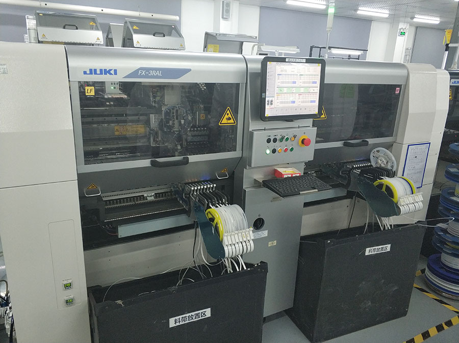
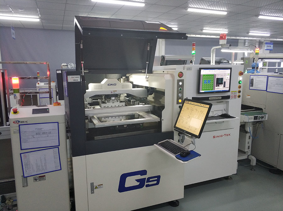
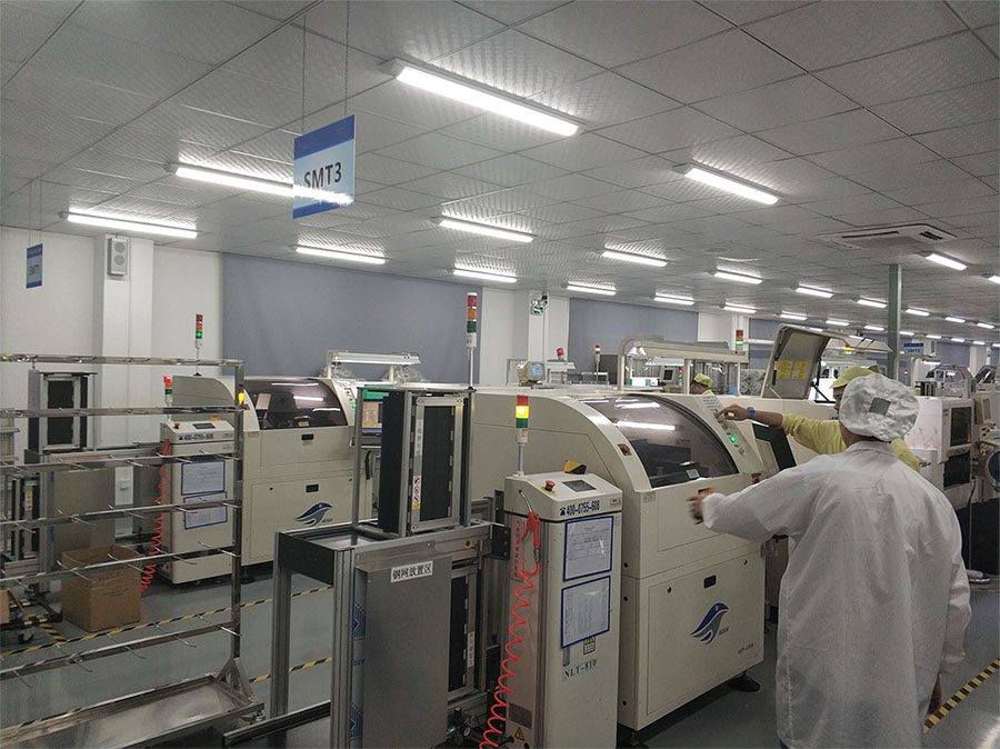
Operating in the heart of Shenzhen's elite electronics corridor, Shenzhen VUKO Electronics Co., Ltd. empowers global OEMs, lighting designers, and industrial hardware innovators to transition seamlessly from rapid prototyping to high-volume production without supply chain fragmentation. Our facilities unite raw board fabrication, turnkey BOM sourcing, SMT assembly, and rigorous functional validation under one coordinated roof.
Direct technical answers to the most common queries raised by hardware engineers and international procurement specialists.
For standard commercial lighting (downlights, fluorescent tube replacements under 15W), a 1.0 to 1.5 W/m·K dielectric layer is cost-effective and reliable. High-power outdoor luminaires, industrial high-bays, architectural floodlights, and automotive projection headlights (above 20W to 150W per module) mandate 2.0 to 5.0 W/m·K dielectric materials or direct thermal path (thermoelectric separation) copper-core constructions to restrict junction temperature (Tj) below 85°C.
Yes, but it depends on the structural configuration. Single-layer aluminum PCBs feature copper traces only on one side and a solid aluminum backer, preventing SMT on the rear. Double-sided MCPCBs incorporate a center aluminum core sandwiched between two dielectric layers and copper foils, or a double-sided circuit layer laminated onto one side of an insulated aluminum base plate. For high density, hybrid rigid-flex or FR4-aluminum bonding is implemented.
The optical reflectivity of the top solder mask directly impacts system lumen output. Specialized ultra-white LED solder masks achieve over 88% to 92% optical reflectivity in the 420-700 nm visible spectrum. Standard green, black, or low-grade white inks yellow and degrade under continuous UV and thermal cycling, absorbing up to 15% of radiant light energy and accelerating lumen depreciation.
Shenzhen VUKO Electronics Co., Ltd. conducts 100% Hi-Pot (Dielectric Withstanding Voltage) testing on all production batches. Depending on class-I or class-II insulation requirements, dielectric thicknesses between 75µm and 150µm are validated against breakdown thresholds ranging from 3000V AC to 6000V DC, complying with UL 796, UL 94V-0 flammability ratings, and CE/RoHS environmental directives.
Warping (bow and twist) typically stems from mismatched Coefficients of Thermal Expansion (CTE) between the copper layer (17 ppm/°C), dielectric resin polymer (30-60 ppm/°C), and aluminum alloy base (23-24 ppm/°C) during reflow soldering exceeding 245°C. Delamination results from substandard prepreg pressing, surface micro-voids, or moisture entrapment. VUKO prevents this via vacuum laminating presses, post-cure baking cycles, and panelized V-scoring balance.
Upload your Gerber files (RS-274X), panel array schematics, and component BOM. Our senior thermal engineering team in Shenzhen will complete a full DFM evaluation and provide a transparent, factory-direct quotation within 24 hours.
Fast-track your procurement RFQ directly to our project managers.
Get a Quote