High-TG HDI PCB Assembly: Engineering Guide, Thermal Reliability, & Turnkey SMT Manufacturing Solutions
Addressing critical procurement inquiries raised by global AI hardware, aerospace, telecommunications, and automotive engineering teams: How to master thermal stress, maintain microvia barrel integrity, prevent BGA warpage, and guarantee IPC Class 3 precision in complex High-TG High Density Interconnect PCB assemblies.
Why High-TG Materials Are Mandatory for HDI Assemblies
Modern dense computing hardware demands tighter line widths, laser-drilled microvias, and fine-pitch BGAs. Without high glass transition temperatures, thermal cycling easily causes catastrophic structural failure.
The Physics of Thermal Modulus in Multi-Reflow Cycles
When electronics manufacturers assemble High Density Interconnect (HDI) boards, the assembly passes through high-temperature zones repeatedly: top-side SMT, bottom-side SMT, through-hole selective soldering, underfill curing, and potential rework. Typical lead-free SAC305 reflow profiles reach peak temperatures between 245°C and 260°C. Standard FR4 base laminates possess a glass transition temperature (Tg) of 130°C to 140°C. Once temperatures exceed Tg, the epoxy resin transitions from a rigid, glassy state into an amorphous rubbery state.
This state transition causes an exponential increase in the material's Coefficient of Thermal Expansion along the Z-axis (CTE-Z). In an HDI architecture packed with microvias, stacked laser vias, and copper-plated through-holes, excessive Z-axis expansion places enormous tensile stress on copper barrels and pad junctions. The consequences are microvia corner cracking, pad lifting under Ball Grid Arrays (BGAs), and inner-layer separation that escape basic functional testing only to fail in the field.
By specifying High-TG materials (Tg ≥ 170°C to 180°C) such as Shengyi S1000-2, ITEQ IT-180A, or Isola 370HR, the resin retains dimensional stability across higher thermal plateaus. High-TG laminates exhibit higher decomposition temperatures (Td ≥ 345°C), prolonged time-to-delamination (T288 ≥ 15 minutes), and significantly reduced Z-axis thermal expansion (typically < 2.5% expansion from 50°C to 260°C). This ensures that ultra-fine laser microvias and solder joints survive grueling industrial operations.
| Property Specification | Standard FR-4 | Mid-TG FR-4 | High-TG FR-4 (VUKO Standard) |
|---|---|---|---|
| Glass Transition Temp (Tg) | 130°C – 140°C | 150°C | 170°C – 180°C |
| Decomposition Temp (Td) | ~300°C | ~320°C | ≥ 345°C – 355°C |
| Z-Axis CTE (Before / After Tg) | 60 / 300 ppm/°C | 50 / 260 ppm/°C | 35–45 / 200–240 ppm/°C |
| Time to Delamination (T288) | 0 – 2 min | 2 – 5 min | ≥ 15 – 30 min |
| Lead-Free SMT Compatibility | High Risk / Poor | Moderate | Optimal / Multi-Cycle Safe |
| Any-Layer & Stacked Via Safety | Unacceptable | Borderline | Recommended for IPC Class 3 |
Recommended HDI Stack-Up Architecture for High-Reliability PCBA
Shenzhen VUKO Electronics Co., Ltd. recommends tailoring your HDI stack-up to match the exact pitch and escape routing requirements of your primary processor or FPGA:
- 1+N+1 (Type I): Ideal for pitch down to 0.65 mm. Outer microvia layer over a rigid core with buried mechanical vias. Cost-effective for edge computing and industrial gateways.
- 2+N+2 (Type II / Staggered or Stacked): Suitable for 0.5 mm to 0.4 mm BGA escape routing. Laser microvias on two outer layers with copper filling (VIPPO). Stacked microvias require High-TG core and prepreg to resist tensile stress.
- Any-Layer HDI (ELIC - Every Layer Interconnect): 8 to 16+ layers composed entirely of laser-drilled, copper-filled microvias. Essential for ultra-miniaturized medical sensors, multi-sensor cameras, and 5G mmWave sub-assemblies.
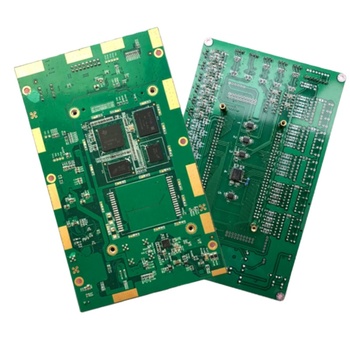
High-TG HDI Prototype & Production Capability
Laser microvias down to 0.075 mm, trace/space 2.5/2.5 mil, high-Tg Shengyi/ITEQ materials, and copper-filled via-in-pad (VIPPO) for seamless 0.35 mm pitch BGA placement.
Send an Inquiry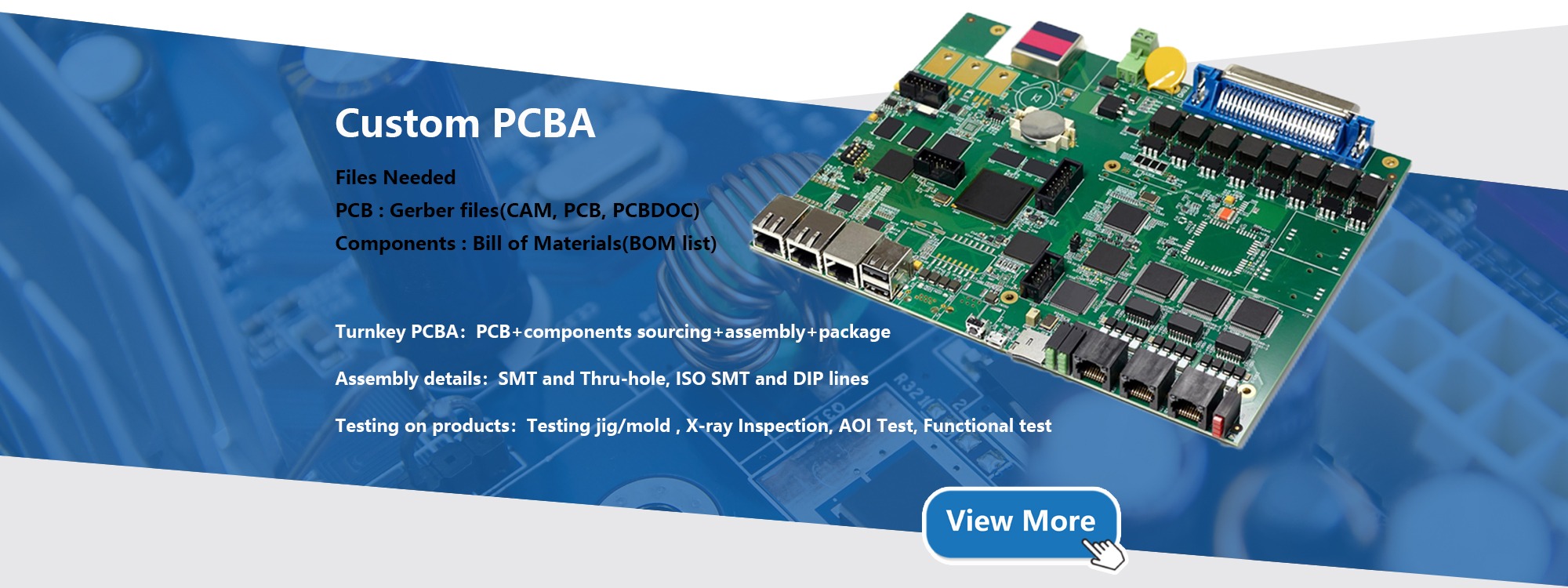
Precision Surface Mount Assembly
Equipped with 3D SPI, multi-zone nitrogen reflow, 3D AXI (X-ray), and AOI inspection. We achieve voiding under 10% on thermal and ground BGA balls.
Send an InquiryThermal Endurance
High-TG substrates (Tg ≥ 170°C) prevent copper track lifting, barrel fractures, and pad cratering throughout lead-free multi-zone reflow profiles.
Ultra-Fine Pitch SMT
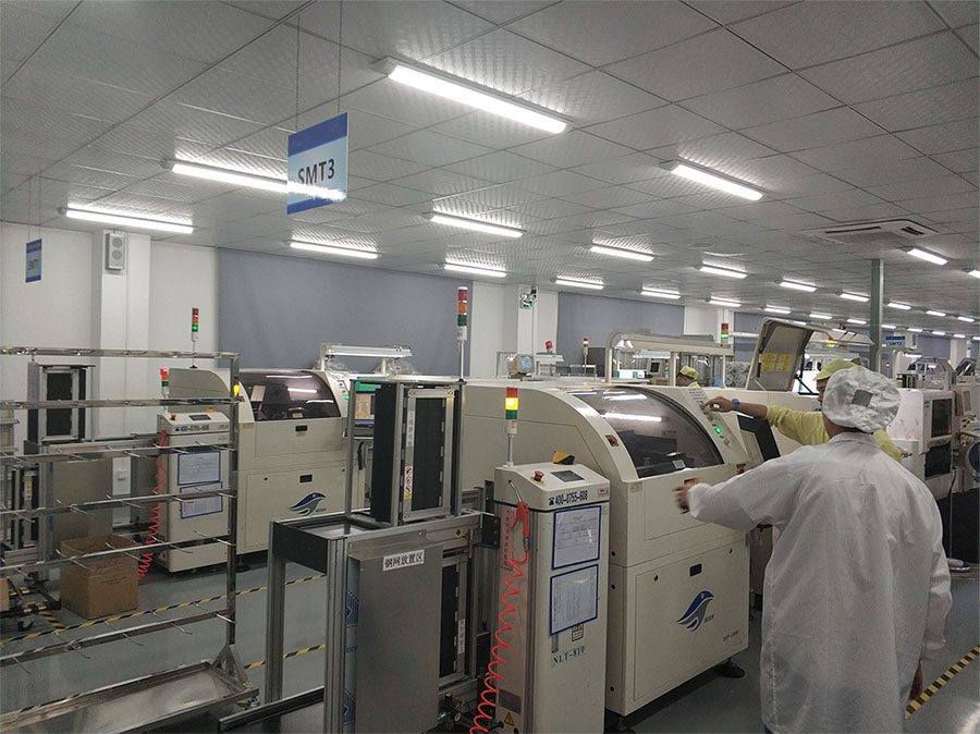
Automated high-speed mounters place 01005 passives and 0.35 mm pitch BGA packages with vacuum de-airing reflow and minimal solder voiding.
Rigorous 3D AXI & AOI
Every HDI assembly is inspected with inline 3D automated optical and 3D radiographic X-ray systems to catch head-in-pillow, bridging, or insufficient fill.
Future Procurement & Technological Trends in High-TG HDI PCBA
Understanding shifting technical standards, AI edge-computing demands, and supply chain strategies allows procurement directors to protect yields and margins.
1. Proliferation of Edge AI Accelerators and Dense PoP Packaging
The shift toward distributed on-device AI processing requires hardware engineers to squeeze high-TFLOPS neural processing units (NPUs) into ultra-compact form factors. This drives widespread adoption of Package-on-Package (PoP) and ultra-fine-pitch BGA devices (0.4 mm to 0.35 mm pitch). Consequently, procurement specifications increasingly mandate 3+N+3 and Any-Layer HDI stack-ups featuring Tg180 laminates to withstand the extreme thermal densities (over 85°C continuous junction temperatures) generated by continuous machine learning inferencing.
2. Transition to Modified Semi-Additive Processes (mSAP)
Conventional subtractive etching hits physical limits when trace width and spacing drop below 50 µm (2 mil), causing trapezoidal conductor shapes and signal degradation at high frequencies. Global OEM buyers are rapidly qualifying manufacturing partners capable of mSAP processing. Using thin electroless copper foils with additive pattern plating produces near-vertical trace sidewalls, tighter impedance tolerances (±5%), and reduced insertion losses for 56Gbps+ SerDes lines.
3. Single-Source Turnkey SMT Procurement to Mitigate Yield Liability
Separating bare HDI fabrication from SMT assembly is becoming obsolete due to warranty friction. If a fine-pitch microvia fails or delaminates under a $400 processor during SMT, bare-board fabricators blame the assembly profile, while assembly houses blame substrate quality. Procurement directors are standardizing on integrated turnkey partners like Shenzhen VUKO Electronics Co., Ltd. that manage DFM, board fab, active BOM component kitting, and SMT under one roof with single-point accountability.
4. Low-Loss / High-TG Hybrid Dielectric Material Blends
Future procurement requires cost optimization through hybrid stack-ups. Instead of fabricating entire 12-layer boards from expensive high-frequency PTFE/hydrocarbon materials, engineering designs now specify hybrid laminations: high-speed signal layers fabricated on low-loss materials (such as Rogers RO4350B or Megtron 6) mated with cost-effective High-TG FR-4 for internal power and ground distribution. Balancing dielectric constants (Dk) and dissipation factors (Df) while preventing thermal expansion mismatches represents the frontline of modern PCB manufacturing.
Technical Capabilities for High-TG HDI Fabrication & Assembly
Engineered to meet IPC-A-600 and IPC-A-610 Class 2 and Class 3 reliability standards across high-density applications.
| Manufacturing Parameter | Standard Capability | Advanced / HDI Capability |
|---|---|---|
| Base Laminate Glass Transition (Tg) | Tg 150°C (Mid-TG FR-4) | Tg 170°C – 180°C (Shengyi, ITEQ, Isola 370HR) |
| HDI Build-Up Architecture | Type I (1+N+1) | Type II (2+N+2), Type III (3+N+3), Any-Layer (ELIC) |
| Layer Count | 4 to 12 Layers | Up to 24 Layers Multilayer HDI |
| Laser Microvia Diameter | 0.10 mm (4 mil) | 0.075 mm (3 mil) UV / CO2 Laser |
| Mechanical Drill Via Size | 0.20 mm (8 mil) | 0.15 mm (6 mil) High-Speed Spindle |
| Aspect Ratio (Laser Microvia) | 0.8:1 | 1:1 (Fully Copper Filled / VIPPO) |
| Min Line Width / Line Space (L/S) | 0.075 / 0.075 mm (3/3 mil) | 0.050 / 0.050 mm (2/2 mil) via mSAP |
| BGA Component Pitch (SMT) | 0.50 mm Pitch | Down to 0.35 mm Pitch BGA & CSP |
| Smallest Discrete Component | 0201 Imperial (0603 Metric) | 01005 Imperial (0402 Metric) Passives |
| Surface Finish Options | Lead-Free HASL, OSP | ENIG (Electroless Nickel Immersion Gold), ENEPIG, Immersion Silver |
| Controlled Impedance Tolerance | ±10% | ±7% standard (±5% upon engineering sign-off) |
| Inspection & Verification | AOI + Electrical E-Test (Flying Probe) | 3D SPI + 3D AOI + 3D Radiographic AXI + Thermal Stress E-Test |
Why Global Hardware Innovators Partner with VUKO Electronics
Based in the epicenter of the global electronics supply ecosystem, Shenzhen VUKO Electronics Co., Ltd. delivers true turnkey manufacturing agility.
Shenzhen VUKO Electronics Co., Ltd.
Since our establishment in Shenzhen, China, Shenzhen VUKO Electronics Co., Ltd. has evolved into an agile, highly reliable hardware manufacturing partner for OEM brands, industrial innovators, and electronic research institutions across 65+ countries. We eliminate the operational overhead of fragmented supply chains by unifying bare board fabrication, strategic BOM component sourcing, high-speed SMT assembly, and rigorous validation under one roof.
Our engineering division reviews every design package prior to tooling. By auditing Gerber layers, netlists, and centroid coordinates against our High-TG manufacturing constraints, we detect subtle design-for-manufacturability (DFM) discrepancies—such as un-vented planes, insufficient microvia land rings, or uneven copper balance—before panels hit the chemical line.
- End-to-End High-TG & HDI Specialization From quick-turn 2-stage laser microvia prototypes to volume production runs with complete impedance traceability.
- Turnkey BOM Component Sourcing & Counterfeit Prevention Procurement via franchise distributors and authorized vendors. We conduct incoming microscope inspections and electrical lot spot checks.
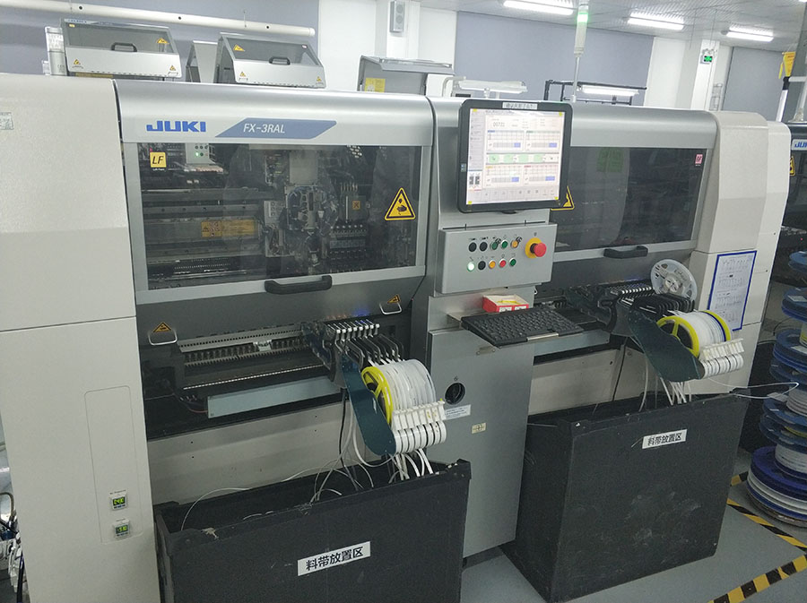
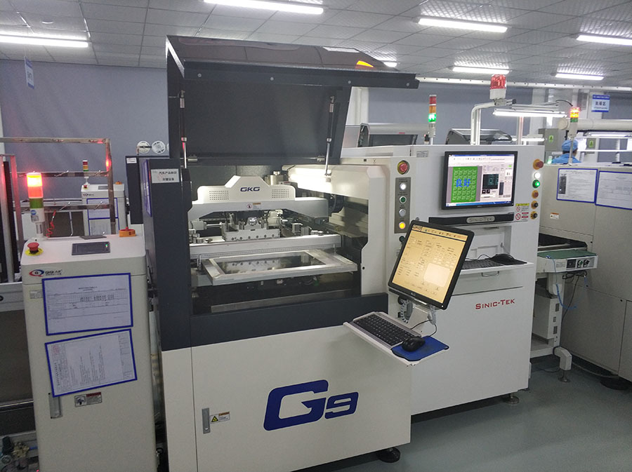
- State-of-the-Art Surface Mount Equipment High-speed Fuji and Yamaha pick-and-place lines, nitrogen reflow ovens, and electroformed nano-coated stencils for ultra-fine BGAs.
- Full HMI & Functional System Integration Beyond rigid HDI, we build custom FPC flex interconnects, aluminum power boards, and tactile membrane switch user interfaces.
- Trade Assurance & Protected Global Shipping Secure escrow payment backing through Alibaba.com Trade Assurance with ESD-safe vacuum packaging and tracked express delivery.
Have an HDI Design Ready for Review?
Upload your Gerber files and bill of materials. Our engineering staff will supply a free DFM check and detailed quote.
Send an InquiryHDI Fabrication & Surface Mount Operations
An inside look at our laser drilling, electroplating, cleanroom imaging, and automated optical testing facilities in Shenzhen.








Standardized Quality & Process Assurance
Our manufacturing and assembly systems operate strictly in accordance with recognized international manufacturing directives.
ISO 9001
Certified quality management workflows
UL 94V-0
Strict flame-retardant certification
RoHS
100% lead-free & hazardous chemical free
IPC Class 3
High-reliability electronic assemblies
Verified Supplier
Onsite factory verification
Trade Assurance
Payment escrow and delivery protection
High-TG HDI PCB Assembly Procurement FAQ
Answers to the top technical and supply chain questions searched by hardware engineers and purchasing managers.
What is High-TG HDI PCB Assembly, and why is Tg crucial for HDI structures?
High-TG HDI PCB Assembly refers to the fabrication and high-precision surface mount assembly of High Density Interconnect circuit boards manufactured using laminates with a Glass Transition Temperature (Tg) of 170°C or higher (commonly Tg170 to Tg180). In HDI structures featuring laser microvias, stacked/staggered blind vias, and ultra-fine trace geometries, controlling the Coefficient of Thermal Expansion along the Z-axis (CTE-Z) is critical.
Standard FR4 (Tg 130°C–140°C) softens and expands dramatically at lead-free reflow temperatures (245°C–260°C). This thermal expansion causes massive tensile stress on copper plating inside tiny laser microvias, leading to barrel fractures, pad lifting, and delamination. High-TG materials preserve their structural stiffness, keeping Z-axis expansion below 2.5% across multiple soldering passes and protecting the integrity of fine-pitch BGA pads.
What microvia architectures and build-up structures does VUKO manufacture?
Shenzhen VUKO Electronics Co., Ltd. produces full-spectrum HDI build-up architectures:
- Type I (1+N+1): Microvias on outer layers over a mechanically drilled core.
- Type II (2+N+2): Dual outer laser-drilled microvia layers, supporting both staggered and stacked configurations.
- Type III (3+N+3): Three consecutive laser microvia dielectric layers, ideal for dense multi-bus routing and tightly pitched processor fan-outs.
- Any-Layer HDI (ELIC): Full interconnect across all layers using solid copper-filled laser microvias, offering maximum routing freedom in handheld and ultra-miniature systems.
We execute laser hole drilling down to 0.075 mm (3 mil) with electroplated copper via fill (VIPPO) for flat solderable pads.
How does VUKO prevent solder voids and head-in-pillow defects under ultra-fine BGAs?
We implement an integrated quality protocol across paste deposition, component placement, and reflow profile management:
- Stencil Technology: We deploy laser-cut, electroformed stencils with hydrophobic nano-coatings to ensure 100% paste aperture release down to 0.35 mm pitch.
- 3D SPI: Inline 3D Solder Paste Inspection evaluates 100% of pads for height, volume, and bridging prior to pick-and-place.
- Atmospheric Nitrogen Reflow: Controlled N2 reflow soldering minimizes oxidation, improves solder wetting, and lowers void rates inside BGA balls to well under 10-15%, adhering to IPC-A-610 Class 3 criteria.
- 3D Radiographic AXI: X-ray inspection inspects hidden solder joints for voids, micro-bridging, and head-in-pillow anomalies.
What substrate brands and dielectric grades do you support for High-TG builds?
We utilize authentic, factory-certified base laminates from industry-leading manufacturers. Our primary materials include Shengyi S1000-2 / S1000-2M (Tg 170°C, high CTI), ITEQ IT-180A / IT-180TC (low CTE, halogen-free options), and Isola 370HR (Tg 180°C, high CAF resistance). For hybrid designs requiring high-frequency RF transmission lines alongside dense digital logic, we integrate Rogers 4350B or Panasonic Megtron laminates with high-Tg FR-4 cores. Every incoming laminate lot includes certificates of analysis (CoA).
How does turnkey BOM sourcing work, and how are component counterfeits prevented?
Our procurement office is located in Shenzhen, providing immediate access to authorized distribution channels. When you submit your BOM with complete Manufacturer Part Numbers (MPNs) and approved secondary vendors (AVL), our kitting team procures directly from verified global franchised distributors (e.g., Digi-Key, Mouser, Arrow, Element14) and verified original component manufacturers.
Components undergo incoming quality control (IQC) including packaging seal verification, date code audits, pin co-planarity checks, and optical microscopy. For high-risk or allocated active ICs, decapsulation and X-ray die verification can be arranged upon request.
What files are required to obtain a formal DFM review and quotation?
To receive a comprehensive engineering DFM audit and quotation within 24 hours, please share:
- Gerber / ODB++ Files: Comprehensive RS-274X or ODB++ dataset including all copper layers, solder masks, silkscreens, drill files, and fabrication drawings detailing dielectric layer stack-ups.
- BOM (Bill of Materials): Excel format listing item numbers, reference designators, quantity, exact MPNs, manufacturer names, component package footprints, and acceptable alternates.
- Pick-and-Place (Centroid) File: ASCII/X-Y coordinate data showing reference designator, pin center positions, and component rotation angles.
- Testing & Quality Specifications: Programming instructions, functional test guidelines, test fixture specifications, or conformal coating requirements.
Ready to Fabricate & Assemble Your High-TG HDI Board?
Partner with Shenzhen VUKO Electronics Co., Ltd. for turnkey manufacturing excellence. Receive an engineering DFM audit and custom quotation within 24 hours.
- Tg170°C / Tg180°C base laminates
- 0.075 mm microvias & VIPPO copper fill
- 01005 & 0.35 mm BGA SMT placement
- Full turnkey BOM procurement in Shenzhen