Alibaba.com Onsite-Verified Supplier Trade Assurance Order Protection [email protected]
🇺🇸 English🇩🇪 Deutsch 🇪🇸 Español🇫🇷 Français 🇵🇹 Português🇮🇹 Italiano 🇷🇺 Русский🇯🇵 日本語 🇰🇷 한국어🇸🇦 العربية 🇹🇷 Türkçe🇳🇱 Nederlands
RF & Microwave Engineering Guide

How to Procure High Frequency Multilayer PCB Boards: The Complete Engineering & Sourcing Specification Guide

Navigating dielectric constant ($D_k$) stability, ultra-low dissipation factors ($D_f$), copper foil roughness, and cost-optimized hybrid stackups for 5G mmWave, ADAS automotive radar, satellite communications, and AI computing hardware.

Get a Quote Explore Substrates
Up to 110 GHzOperating Frequency
±5%Impedance Tolerance
2–32 LayersMultilayer Stackups
24hDFM Turnaround
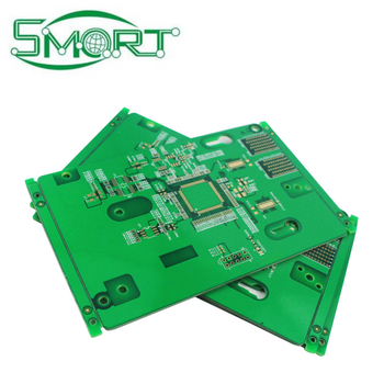
High Frequency Multilayer PCB Board manufactured by Shenzhen VUKO Electronics Co., Ltd.
Substrate Families:Rogers, Taconic, Isola, Megtron
Dielectric Constant ($D_k$):2.15 to 10.2 (±0.05)
Dissipation Factor ($D_f$):0.0009 to 0.0035 @ 10 GHz
Core Construction:Homogeneous PTFE / Hybrid FR-4
Surface Metallurgy:ENEPIG, Immersion Ag, Pure OSP
Production Location:Shenzhen, China (Full Turnkey)
RF Signal Integrity & Material Science

Critical Engineering Parameters in High Frequency Multilayer Boards

Designing and sourcing high frequency multilayer PCBs demands a rigorous understanding of high-speed physics. Unlike standard FR-4 circuit boards, RF and microwave boards treat copper traces not merely as simple conductors, but as distributed transmission lines where every physical boundary dictates insertion loss, phase jitter, and signal attenuation.

Dielectric Stability

Dielectric Constant ($D_k$) & Tolerance

Variations in dielectric constant cause direct phase distortion and characteristic impedance mismatch. At millimeter-wave bands (24 GHz to 77 GHz), an unintended shift of ΔDk = 0.1 shifts a microstrip trace impedance by several ohms, causing signal reflection and VSWR degradation.

  • Tight laminate tolerances down to ±0.02
  • Thermal Coefficient of Dielectric Constant (TCDk) < 50 ppm/°C
  • Homogeneous resin-to-glass ratio across layers
Loss Minimization

Dissipation Factor ($D_f$) & Attenuation

Dielectric loss is linearly proportional to operating frequency. As frequencies climb into the gigahertz realm, materials with a high loss tangent generate thermal heat and severely degrade signal reach. Specialized PTFE and hydrocarbon resins maintain signal strength across multi-gigabit backplanes.

  • Ultra-low $D_f$ down to 0.0009 at 10 GHz
  • Low moisture absorption (<0.06%) preventing water losses
  • Optimized eye-diagrams for 56G/112G PAM4 lines
Conductor Dynamics

Copper Foil Roughness & Skin Depth

Due to the skin effect, high frequency currents travel strictly along the outer perimeter of the conductor. If copper surface teeth (profile height Rz) exceed the skin depth, current paths become physically elongated, dramatically escalating resistive conductor loss.

  • HVLP (Hyper Very Low Profile) copper foils
  • Rolled Annealed (RA) foils for demanding radar traces
  • Treated Reverse Treated Foils (RTF) for fine lines
Material Selection Guide

High Frequency Multilayer Substrates: Engineering Comparison

Selecting the proper laminate balance between electrical performance, thermal endurance, and bill-of-materials cost is the most crucial decision during RF procurement.

Substrate Material Dielectric Constant (Dk @ 10 GHz) Dissipation Factor (Df @ 10 GHz) Thermal Conductivity (W/m·K) Glass Transition Temp (Tg) Ideal Procurement Application
Rogers RO4350B
Hydrocarbon / Ceramic
3.48 ± 0.05 0.0037 0.69 >280 °C 5G Base Stations, Power Amplifiers, Hybrid Multilayers Cost-Effective
Rogers RO3003
Ceramic-filled PTFE
3.00 ± 0.04 0.0010 0.50 N/A (PTFE) 77 GHz Automotive Radar, mmWave Antennas Ultra-Low Loss
Taconic TLX-8
PTFE Fiberglass
2.55 ± 0.04 0.0017 0.42 N/A (PTFE) Aerospace Radar, Phased Array, Couplers
Panasonic Megtron 6
High-Tg Low Loss PPE
3.71 0.0020 0.40 185 °C AI Server Backplanes, PCIe 5.0/6.0, 400G Optical Switches
Isola Astra MT77
Modified Low-Loss FR-4 resin
3.00 0.0017 0.45 200 °C High-Density Hybrid Multilayers, Satellite Radio
Standard High-Tg FR-4
(Baseline comparison)
4.40 ± 0.20 0.0180 0.30 170 °C DC Bias, Control Layers & Digital Low-Speed Support
Why Choose VUKO

Enterprise Manufacturing Strengths & Fabrication Authority

Shenzhen VUKO Electronics Co., Ltd. combines more than 14 years of verified manufacturing mastery with direct access to Shenzhen's world-class electronics supply chain ecosystem.

Alibaba.com Onsite-Verified Supplier & 14+ Years Export Track Record

Shenzhen VUKO Electronics Co., Ltd. has served international tier-1 hardware brands, telecom innovators, and industrial engineering enterprises across 60+ countries with complete Trade Assurance order security.

Precise Impedance Control & VNA Testing Capability

Equipped with state-of-the-art Vector Network Analyzers (VNA) and Time Domain Reflectometry (TDR) test stations, ensuring characteristic impedance tolerances within ±5% across single-ended microstrip, coplanar waveguide, and differential pair traces.

Rapid Engineering DFM & Prototype Delivery

Receive an actionable Design for Manufacturability review within 24 hours of Gerber submission. Quick-turn prototypes delivered in as fast as 3 to 5 business days, scaling smoothly into mass volume.

One-Stop Turnkey Ecosystem: PCB, PCBA, FPC & Sourcing

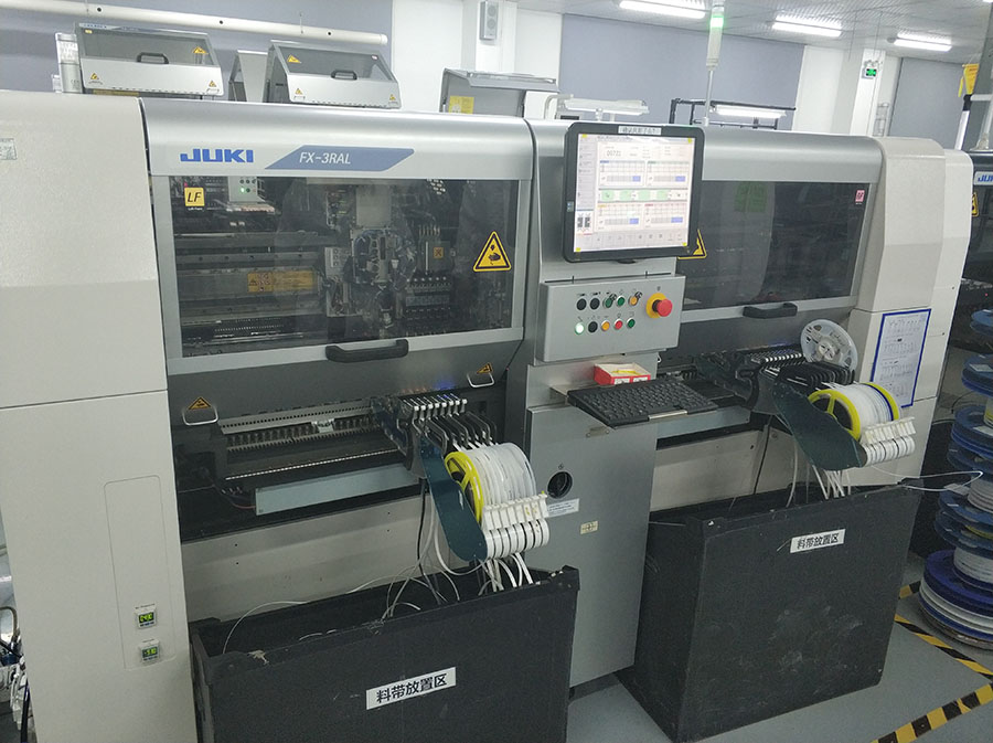
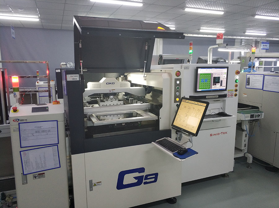
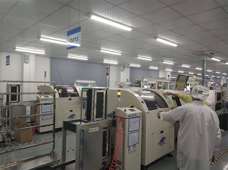
Beyond bare RF boards, our facility offers turnkey SMT assembly with 01005 component capabilities, x-ray inspection for BGA/QFN packaging, IC programming, and full BOM electronic component procurement under one roof.

Procurement FAQ

Frequently Asked Questions on High Frequency Multilayer Boards

Crucial answers to the most common engineering and procurement inquiries raised by global hardware engineers and sourcing managers.

How do Dk and Df tolerances impact high frequency multilayer PCB performance?

Dielectric constant ($D_k$) stability dictates electrical signal propagation velocity and phase consistency across circuit traces, while the dissipation factor ($D_f$ or loss tangent) determines signal attenuation and dielectric loss. In high frequency multilayer PCBs operating above 5 GHz, small variations in $D_k$ distort signal timing and impedance, while elevated $D_f$ causes excessive thermal dissipation and signal degradation. Tight lamination tolerances (such as $D_k$ held within ±0.05) ensure consistent characteristic impedance and minimal signal decay along critical RF feeds.

Why are hybrid multilayer stackups (Rogers + FR-4) widely preferred over pure RF laminates?

Hybrid multilayer stackups combine high-frequency laminates (such as Rogers RO4350B or RO4003C) on the outer signal layers with standard mid/high-Tg FR-4 prepreg and cores for the internal digital, ground, and DC power distribution planes. This hybrid construction cuts substrate raw material expenses by 30% to 50%, improves mechanical rigidity, mitigates z-axis thermal expansion mismatch, and simplifies standard multilayer lamination cycles without compromising critical RF performance.

What surface finishes are optimal for high-frequency RF boards to avoid skin effect losses?

At high frequencies (10 GHz to 77 GHz), electromagnetic signals travel primarily along the outer periphery of copper traces due to the skin effect. Finishes containing nickel, such as standard Electroless Nickel Immersion Gold (ENIG), can introduce ferromagnetic loss and higher signal attenuation. Optimal finishes include Immersion Silver (IAg), Electroless Nickel Electroless Palladium Immersion Gold (ENEPIG), or direct Bare Copper with Organic Solderability Preservative (OSP), which offer smooth conductor boundaries and minimal insertion losses.

How does copper foil roughness affect high frequency signal transmission?

As signal frequencies enter the microwave and millimeter-wave domains, the skin depth drops below 1 micron. When copper surface roughness ($R_z$ or $R_a$) exceeds or approaches the skin depth, high-frequency currents are forced through circuitous paths, drastically increasing resistive conductor loss and phase delay. High frequency multilayer PCBs require Very Low Profile (VLP) or Hyper Very Low Profile (HVLP/RTF) treated copper foils to preserve eye-diagram integrity and minimize insertion loss.

What verification and testing procedures are essential for high frequency multilayer boards before shipment?

Critical RF verification includes Time Domain Reflectometry (TDR) for differential and single-ended characteristic impedance verification (tested on specialized impedance coupons down to ±5%), Vector Network Analyzer (VNA) testing for S-parameter and insertion loss measurements, micro-sectioning to inspect copper plating thickness and PTH barrel integrity, and automated optical inspection (AOI) coupled with flying probe electrical testing to prevent shorts, opens, and trace neckdowns.

What files and documentation are required to quote a custom high frequency PCB?

To provide a guaranteed quotation and comprehensive DFM review within 24 hours, Shenzhen VUKO Electronics Co., Ltd. requires RS-274X or ODB++ Gerber files, an explicit layer stackup diagram showing dielectric thickness and target impedance values, drill files, surface finish requirements, and notes indicating laminate material preferences (e.g., Rogers 4350B, Taconic, or hybrid constructions).

Accelerate Your High-Frequency Hardware Development

Send your Gerber files, impedance specifications, and BOM today. Our engineering team at Shenzhen VUKO Electronics Co., Ltd. will review your stackup and provide a competitive quotation within 24 hours.