Search Intent Knowledgebase
Frequently Asked Questions: Sourcing & Designing Custom FPC
Clear, direct engineering answers to the most common questions raised by hardware designers, project managers, and strategic buyers.
What is the difference between Rolled Annealed (RA) and Electro-Deposited (ED) copper in FPC fabrication?
The choice between Rolled Annealed (RA) and Electro-Deposited (ED) copper is the single most critical factor in flex circuit mechanical life. RA copper is created by mechanically rolling ingots down to foil thickness; its elongated grain structure provides exceptional ductile endurance, making it mandatory for dynamic flexing applications (such as laptop hinges, camera gimbals, and wearable sensors) requiring over 100,000 flex cycles. In contrast, ED copper possesses a vertical column grain structure formed via electroplating; it provides superior trace adhesion and allows for ultra-fine line etching below 30 µm, making it ideal for static "bend-to-fit" assemblies where the circuit is bent only once during final product enclosure assembly.
How do I calculate and optimize the minimum bend radius for my custom FPC?
To avoid trace cracking and coverlay micro-buckling, IPC guidelines define clear bend radius formulas based on copper type and layer count. For single-sided flex circuits subjected to static installation bends, the minimum bend radius (R) must be at least 6× the overall circuit thickness (T). For double-sided flex, R should be at least 10× T. For dynamic flexing applications, R must be increased to at least 20× to 40× the total thickness. Crucially, copper traces running through bending zones should be routed perpendicularly to the bend axis, trace widths must remain uniform without sharp 90-degree corners, and teardrops should always be added at via-to-trace junctions.
What types of stiffeners can Shenzhen VUKO Electronics Co., Ltd. integrate, and how do they function?
Because flex circuits cannot naturally support heavy components or resist connector insertion friction, localized stiffeners are bonded to the back of the circuit using thermal-setting acrylic or pressure-sensitive adhesive (such as 3M 467MP/9495LE). We offer:
1. Polyimide (PI) Stiffeners: Typically 0.05 mm to 0.225 mm thick; applied behind ZIF connector contact fingers to achieve exact thickness mating specs (e.g., 0.30 mm ±0.03 mm).
2. FR-4 Stiffeners: Ranging from 0.2 mm to 1.6 mm thick; placed under SMT component clusters and BGA areas to prevent solder joints from flexing and shearing off under stress.
3. Stainless Steel / Aluminum Stiffeners: Used in ultra-flat connector regions, heat dissipation pads, and grounding plates requiring absolute coplanarity and mechanical shielding.
How can I prevent flex circuit cracking and micro-fractures during mass SMT reflow?
Polyimide is naturally hygroscopic, absorbing up to 1.5% to 3.0% ambient moisture. If an FPC is processed through reflow soldering without adequate pre-treatment, rapid moisture vaporization causes immediate blister delamination, barrel cracking in plated through-holes (PTH), and solder ball splattering. Shenzhen VUKO Electronics Co., Ltd. eliminates these risks by:
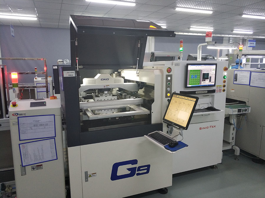
• Baking all bare FPCs in moisture-vacuum baking ovens at 110°C–120°C for 2 to 4 hours immediately prior to solder paste printing.
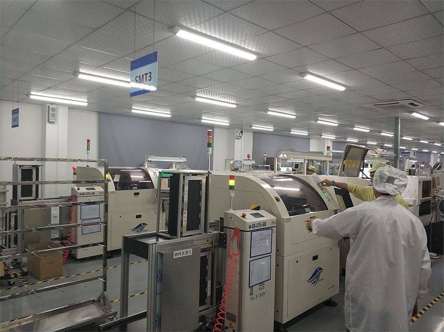
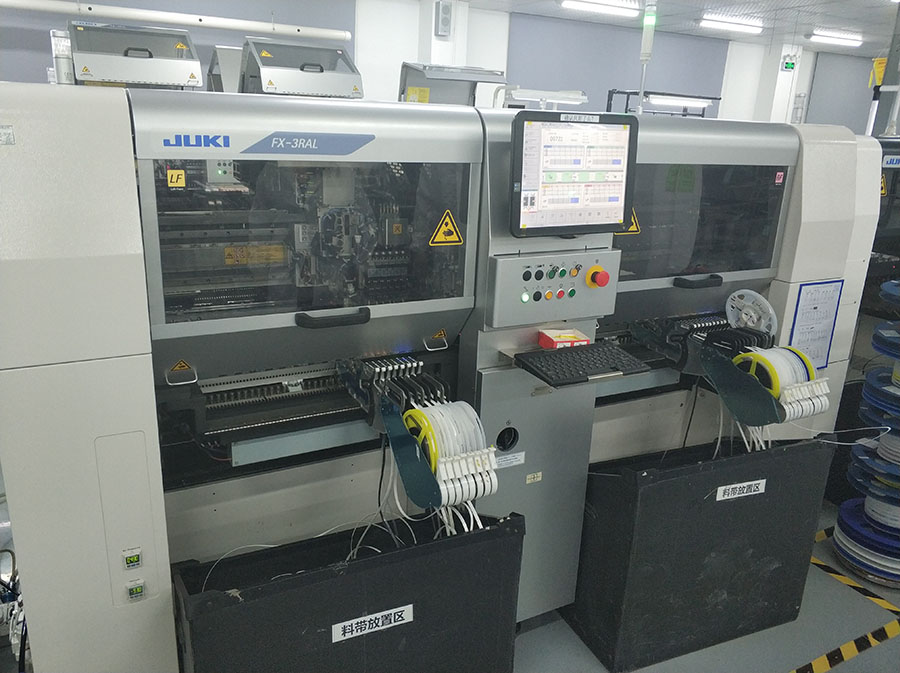
• Mounting flex circuits onto custom high-precision aluminum or synthetic stone magnetic pallet jigs to ensure perfectly flat coplanarity during high-speed SMT component placement.
• Optimizing peak reflow temperatures (typically 240°C–245°C for lead-free SAC305) with gradual pre-heating profiles to prevent thermal shock.
What engineering design package should I provide for an accurate custom FPC quotation?
To provide a firm quotation and comprehensive DFM review within 24 hours, our engineering team requires:
1. Complete Gerber files (RS-274X or ODB++ format) including circuit layers, coverlay opening layers, stiffener outlines, and NC drill files.
2. Mechanical 2D drawing (DXF or PDF) specifying outline tolerances, stiffener thicknesses, golden finger bevel angles, and fold lines.
3. Layer stack-up documentation indicating copper weight (e.g., 18µm or 35µm), base polyimide thickness (12.5µm or 25µm), and surface plating specifications (e.g., ENIG 2u" gold or hard gold).
4. Bill of Materials (BOM) with complete manufacturer part numbers (MPN) if turnkey component sourcing and SMT flex assembly are requested.
What quality inspection protocols are performed on flexible circuit orders before shipment?
Every single production batch at Shenzhen VUKO Electronics Co., Ltd. undergoes comprehensive quality checks:
• 100% Electrical Testing: Flying probe testing for prototypes or dedicated fixture E-test for volume batches to verify zero open/short circuits down to 100V insulation resistance.
• Automated Optical Inspection (AOI): High-resolution optical scanning verifying line widths, spacing, via annular rings, and etch definition.
• Mechanical & Environmental QC: Solder float testing at 260°C for 10 seconds, copper foil peel strength testing (>1.0 N/mm), cross-section micro-section analysis, and dynamic bending cycle qualification.
• Final Visual & Packaging: 100% microscope inspection of surface finish and contact fingers, followed by vacuum ESD protective packaging.