Alibaba.com Onsite-Verified Supplier Trade Assurance Order Protection [email protected]
🇺🇸 English🇩🇪 Deutsch 🇪🇸 Español🇫🇷 Français 🇵🇹 Português🇮🇹 Italiano 🇷🇺 Русский🇯🇵 日本語 🇰🇷 한국어🇸🇦 العربية 🇹🇷 Türkçe🇳🇱 Nederlands
Thermal & High-Current Engineering

Heavy Copper PCB Board Fabrication: The Complete Engineering & Global Procurement Guide

From electric vehicle powertrains to megawatt grid inverters, modern electronics demand severe current conduction and aggressive thermal dissipation. Shenzhen VUKO Electronics Co., Ltd. delivers mission-critical heavy copper PCB fabrication from 3 oz to 30 oz, engineered to eliminate busbars, prevent thermal failure, and maximize MTBF under punishing thermal cycle profiles.

Get a Quote View Technical Matrix
3 oz – 30 oz Finished Copper Weight
TG170 – TG200 High-TG Halogen-Free FR4
IPC Class 2/3 100% E-Test & AOI Verified
Shenzhen VUKO Electronics Heavy Copper Engineering and Inspection Team
Shenzhen VUKO Technical Laboratory Specialized etched trace profiling, multi-pass solder mask curing, and vacuum resin impregnation prevent voiding and delamination in heavy copper circuit board fabrication.
Engineering Insight

Solving the Core Challenges in Heavy Copper PCB Board Fabrication

Global procurement teams and hardware architects often struggle when scaling prototypes with copper thickness above 3 oz. Understanding the underlying manufacturing dynamics prevents costly layout revisions and premature field failures.

Advanced Differential Etching

Etching 4 oz to 10 oz copper foils inherently introduces severe chemical undercut. Standard etching parameters result in trapezoidal trace walls and necking. Shenzhen VUKO Electronics uses synchronized multi-stage chemical etching with proprietary anisotropic additives to maintain steep sidewall geometries and tightly control finished trace impedance and current density.

Void-Free Lamination & Resin Fill

Deep valleys between heavy copper traces make multilayer lamination challenging. Trapped air pockets cause micro-delamination and catastrophic high-voltage arc breakdown. We deploy high-flow, high-resin prepregs (such as 1080/106 RC 70%+) managed under dynamic multi-temperature vacuum press profiles to guarantee 100% solid dielectric encapsulation.

Multi-Pass Solder Mask Deposition

Standard liquid photoimageable (LPI) solder mask cannot bridge the sharp vertical cliffs of thick copper tracks (105 µm to 400 µm). A single pass leaves exposed corners vulnerable to oxidation and dendrite growth. We utilize electrostatic spray coating combined with double-curved multi-pass screen printing to ensure continuous minimum 1.2 mil mask coverage over every trace edge.

Manufacturing Precision

Heavy Copper Technical Specification Matrix

Shenzhen VUKO Electronics Co., Ltd. operates strict IPC-6012 Class 2 and Class 3 manufacturing guidelines across all high-current substrate fabrications.

Parameter Standard Heavy Copper Extreme Heavy Copper VUKO Quality Benchmark
Finished Copper Weight 3 oz / 4 oz / 5 oz (105–175 µm) 6 oz up to 30 oz (210–1050 µm) Strict micro-section verification of outer & inner foil
Layer Count 2 to 16 Layers 1 to 6 Layers Mixed inner/outer copper stackup available
Base Laminates Shengyi S1000-2, ITEQ IT-180A, Nelco High-TG Polyimide, Isola 370HR, Rogers TG ≥ 170°C, Td ≥ 350°C, low Z-axis CTE expansion
Min. Line Width / Spacing 8 mil / 8 mil (0.20 mm / 0.20 mm) for 3 oz 16 mil / 18 mil (0.40 mm / 0.45 mm) for 8 oz+ Laser optical inspection after chemical stripping
Hole Wall Copper Thickness ≥ 25 µm (IPC Class 2) ≥ 35 µm to 50 µm (IPC Class 3) Reinforced through-hole barrel plating under high agitation
Surface Finish Selection Lead-Free HASL, ENIG (Electroless Ni/Au) Immersion Ag, Hard Gold, ENEPIG Flat planar coplanarity for dense power SMT packages
Solder Mask Coverage Dual-coat LPI with customized thermal cure Triple-coat or specialized Taiyo thermal mask Dielectric breakdown > 500 V/mil; zero edge peeling
Electrical Testing Standard Flying Probe Test Dedicated Fixture Clamping + High Pot Test Continuity 100%, isolation 100%, up to 3000 VDC test
Get a Quote
Strategic Procurement

Future Sourcing Trends in Heavy Copper PCB Board Fabrication

As modern power electronics evolve, heavy copper circuit board fabrication is shifting from a simple commoditized board-etching process into an advanced integrated thermal-mechanical discipline.

1. Replacement of Discrete Busbars

Engineers are actively eliminating physical busbars, copper bars, and discrete wire looms. Integrating heavy copper (6 oz to 12 oz) directly into the main multilayer board simplifies assembly, saves internal chassis volume, reduces labor overhead by over 30%, and lowers electromagnetic parasitic inductance.

2. Hybrid Mixed-Weight Stackups

Modern applications require high-speed digital control (microcontrollers, DSPs, CAN transceivers) on the same board as high-current motor drivers or power stages. Sourcing trends favor hybrid stackups where high-copper power planes (e.g., 4 oz) sit beneath standard 1 oz fine-pitch signal routing.

3. Wide Bandgap (GaN/SiC) Adoption

Silicon Carbide (SiC) and Gallium Nitride (GaN) switching components operate at higher switching speeds and elevated thermal thresholds. Heavy copper PCB boards act as primary heat spreaders, transferring junction heat laterally across the plane to chassis heat sinks without bulky external cooling.

4. Circular Economy & Halogen-Free Compliance

Global environmental mandates, including RoHS, REACH, and UL 94V-0 flammability rules, require environmentally inert, lead-free compatible resins. Procuring heavy copper boards manufactured with high-temperature halogen-free laminates guarantees longevity in harsh automotive and marine settings.

Our Core Strengths

Why Tier-1 OEM Engineers Rely on Shenzhen VUKO Electronics

Rooted in Shenzhen’s premier high-technology ecosystem, Shenzhen VUKO Electronics Co., Ltd. blends over a decade of precision export manufacturing with deep material science capabilities.

Shenzhen VUKO Electronics Engineering Management Office

Dedicated DFM Engineering Support

Our veteran CAM engineers conduct complete 24-hour Design For Manufacturability (DFM) audits. We verify copper balance, thermal relief radii, trace clearances, and drill aspect ratios to eliminate field rework before copper hits the chemical line.

Shenzhen VUKO Electronics Sales, Tech Support and Account Planning

Transparent Global Project Coordination

From initial Gerber gerber review to rapid prototype turnarounds and mass rollouts, our project leads provide continuous real-time progress reports, micro-section cross-sectional data, and international logistics coordination.

Shenzhen VUKO Electronics Showroom with Heavy Copper and Multilayer PCB Samples

End-to-End Turnkey Hardware Integration

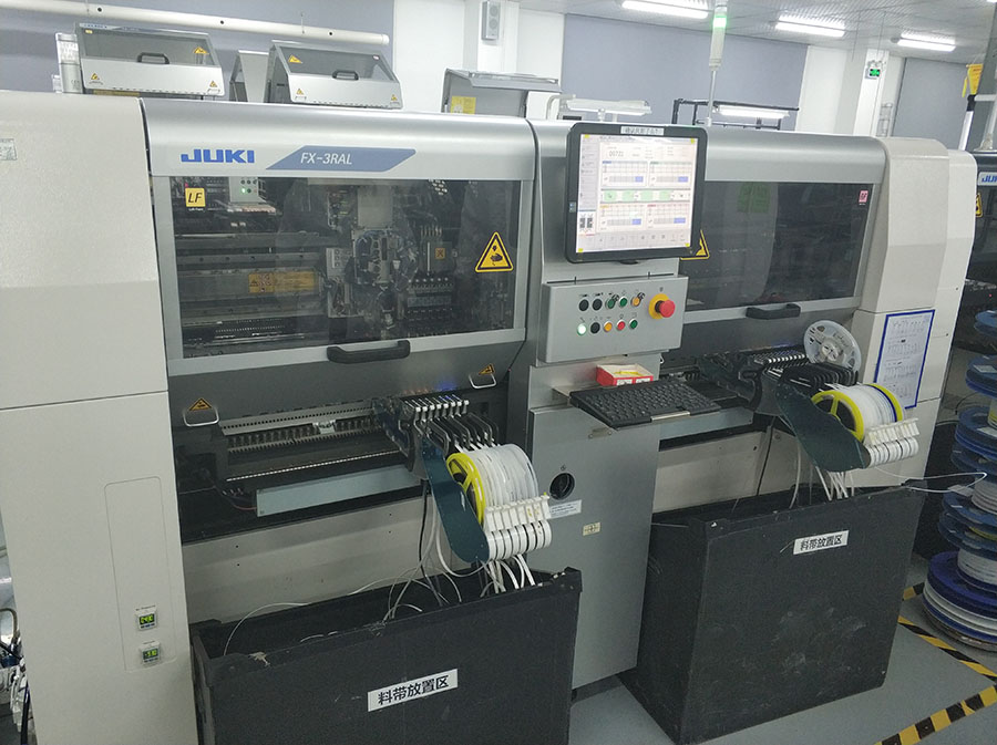
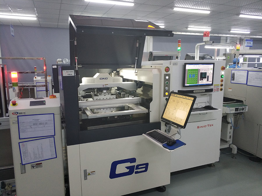
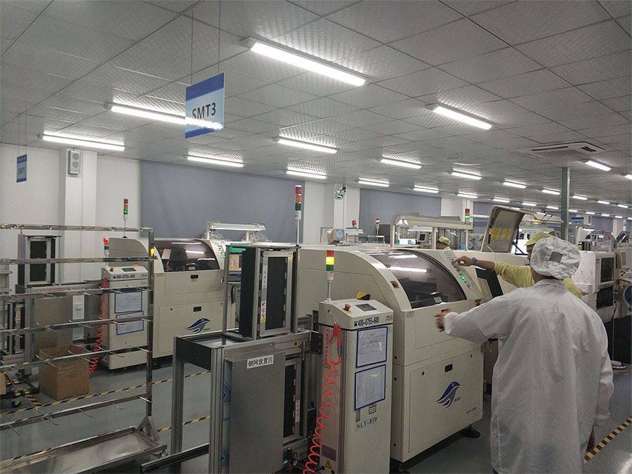
Beyond bare-board heavy copper fabrication, our facility provides turnkey component procurement, high-thermal SMT assembly with solder void monitoring, conformal coating, functional fixtures, and membrane keypad integration under one roof.

Looking for Rapid Prototyping or Mass Heavy Copper Production?

Custom batch orders from 5 pieces with complete raw material traceability certificates (COC, UL, RoHS).

Get a Quote
Frequently Asked Questions

Comprehensive Heavy Copper PCB Board Fabrication FAQ

Real-world engineering questions addressed directly by the Shenzhen VUKO Electronics manufacturing team.

What defines a heavy copper PCB versus a standard PCB?

Standard PCBs typically utilize 0.5 oz to 2 oz copper thickness (18 µm to 70 µm). A Heavy Copper PCB features copper weights from 3 oz/ft² up to 10 oz/ft² (105 µm to 350 µm), with structures reaching 10 oz to 30 oz categorized as extreme heavy copper. Heavy copper boards are designed specifically to carry high currents, manage massive thermal loads, and survive severe thermal cycles without requiring external wiring harnesses or bulky heat sinks.

How do you achieve uniform resin filling during multilayer heavy copper lamination?

Etching thick copper creates steep sidewalls and deep trace valleys. To eliminate voiding, resin starvation, and delamination, Shenzhen VUKO Electronics employs high-resin content prepregs (such as 1080 and 106 high-flow systems) paired with custom vacuum lamination cycle profiling. In extreme thicknesses, differential multi-pass resin paste printing or specialized thermal bonding sheets are applied before secondary hot pressing.

What surface finishes are recommended for heavy copper circuit boards?

Electroless Nickel Immersion Gold (ENIG), Hot Air Solder Leveling (Lead-Free HASL), and Immersion Silver are most commonly specified. ENIG provides excellent surface planarity for fine-pitch SMT components alongside thick copper power traces, while also preventing copper oxidation during high-temperature assembly cycles.

What are the minimum trace width and trace spacing rules for heavy copper fabrication?

Design rules scale directly with copper weight due to chemical undercut during etching. For 3 oz copper, minimum trace and space is typically 8 mil / 8 mil (0.20 mm). For 6 oz copper, it increases to 12 mil / 14 mil (0.30 mm / 0.35 mm). For 10 oz to 12 oz, minimum spacing requirements expand to 16–20 mil (0.40–0.50 mm) to allow proper etchant replenishment and complete chemical clearing.

Can Shenzhen VUKO Electronics combine heavy copper power circuits with fine-pitch signal circuits on the same board?

Yes. Through differential etching techniques and mixed-copper stackups, we integrate heavy copper power circuits (e.g., 4 oz to 8 oz) on outer or inner layers with standard 1 oz or 2 oz control layers. This eliminates the need for discrete busbars and bulky wiring harnesses, consolidating high-current distribution and high-speed MCU/DSP control into a single compact board.

How does heavy copper improve thermal management compared to thermal vias or aluminum MCPCBs?

While aluminum metal-core PCBs are primarily single-sided or restricted in routing density, heavy copper PCBs allow true multilayer interconnectivity. Heavy copper traces conduct heat both horizontally across large surface planes and vertically through heavy-plated through-holes (PTH with 35–50 µm copper barrels), transferring heat directly from power MOSFETs and IGBTs into chassis enclosures.

What files are required to obtain a DFM analysis and fast quotation?

To initiate a quotation, please provide your complete Gerber files (RS-274X or ODB++ format), drill files, fabrication print specifying layer stackup, finished copper thickness per layer, solder mask color, surface finish, board dimensions, panelization arrays, and targeted order quantities. Send your design package to [email protected] or connect directly via our live platform.
Launch Your Heavy Copper PCB Project with Certified Experts

Whether you require a quick-turn prototype run of 5 pieces or volume production for automotive and renewable energy programs, our Shenzhen engineering team is ready to evaluate your layout and deliver optimized thermal performance.

Get a Quote Technical support: [email protected]

24-Hour Engineering DFM Review

Upload your Gerber files and stackup notes. Our team validates line width compensation, aspect ratios, and resin fill ratios before initiating production.

Get a Quote