Precision Electronic Manufacturing & Core Assemblies
Explore our specialized electronic assemblies, thermal management substrates, high-grade interface modules, and PCB fabrication solutions designed for European Original Equipment Manufacturers (OEMs).
CE Certification Rigor: Harmonizing PCB & PCBA for Florence Enterprises
Navigating the stringent electro-technical landscape of the European Union requires absolute transparency at the laminate, solder chemistry, component provenance, and electromagnetic compatibility levels.
EMC Directive (2014/30/EU)
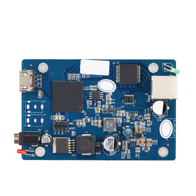
Printed circuit boards deployed across Florence's automated industrial parks and research corridors must exhibit impeccable signal integrity. We implement controlled differential impedance (±5%), solid copper reference ground planes, and specialized decoupling architectures to ensure your end-devices effortlessly conquer CISPR 32 / EN 55032 radiated emissions tests.
Low Voltage Directive (2014/35/EU)
For electronics operating between 50 and 1,000 V AC or 75 and 1,500 V DC, safety is governed by creepage and clearance distances defined by EN 62368-1. We utilize high Comparative Tracking Index laminates (CTI ≥ 600V, CTI 1/0) and IPC-2221 certified track spacing to prevent breakdown voltages and ensure lifelong operational safety.
RoHS 3 (2015/863) & REACH
Environmental compliance within the European Economic Area demands zero compromise on banned hazardous elements. All our raw base materials (Shengyi, ITEQ, Rogers), surface finishes (Lead-Free HASL, ENIG, Immersion Silver), and solder pastes (SAC305) maintain full chemical traceability and come accompanied by ICP laboratory certificates.
Tailored Circuit Architectures for Tuscany’s Leading Sectors
From the scientific laboratories of Sesto Fiorentino to the advanced manufacturing clusters of Scandicci, Campi Bisenzio, and Osmannoro, Florence engineering requires precision-tailored electronic substrates.
Biomedical Instrumentation & Careggi Health Cluster
Florence is internationally celebrated for advanced clinical diagnostics, biomedical optics, and medical device innovation linked to the Careggi University Hospital complex. Medical equipment demands ultra-stable, low-noise multi-layer FR4 boards and fine-pitch Flex-Rigid interconnections capable of enduring chemical cleaning.
Our PCB fabrication maintains IPC Class 3 standards, gold wire-bondable ENIG/ENEPIG finishes, and high-density microvias (HDI laser microvias ≤ 0.1mm) to support ultra-sensitive diagnostic sensor heads, portable hemodialysis control circuitry, and in-vitro optical readers.
Optoelectronics, Photonics & Scientific Research
At the Florence Scientific and Technological Pole (Polo Scientifico di Sesto Fiorentino), high-energy lasers, optical sensors, and astronomical instrumentation are developed daily. These systems generate critical heat densities that directly affect photonic wavelength coherence.
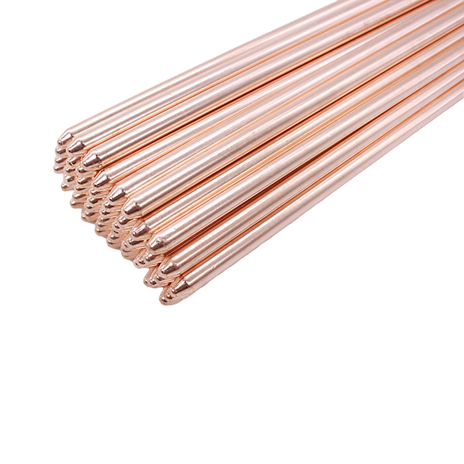
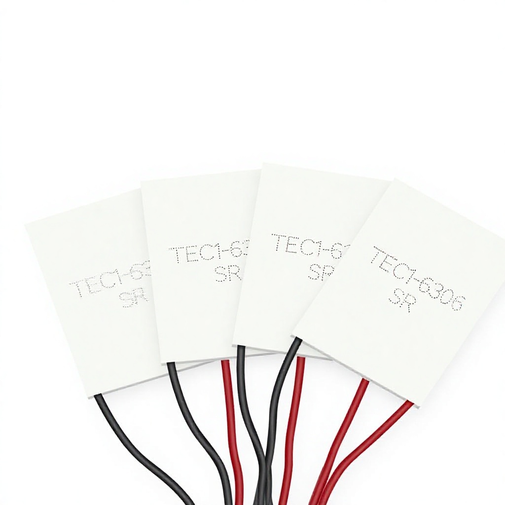
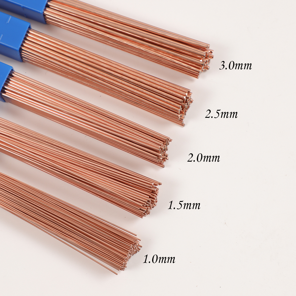
Our solution integrates high-thermal-conductivity Aluminum MCPCBs (1.0 to 5.0 W/m·K), thermoelectric Peltier modules (such as the TEC1-12702), and custom flat sintered copper heat pipes to maintain micro-Kelvin thermal equilibrium on optical sensor arrays and laser pump diodes.
Luxury Goods Automation & CNC Leatherworking (Scandicci)
Scandicci represents the pinnacle of global luxury leather crafting, footwear design, and high-fashion accessory engineering. Modern luxury workshops rely heavily on automated high-speed CNC cutting tables, vision-guided embossing machinery, and robotic stitching cells.
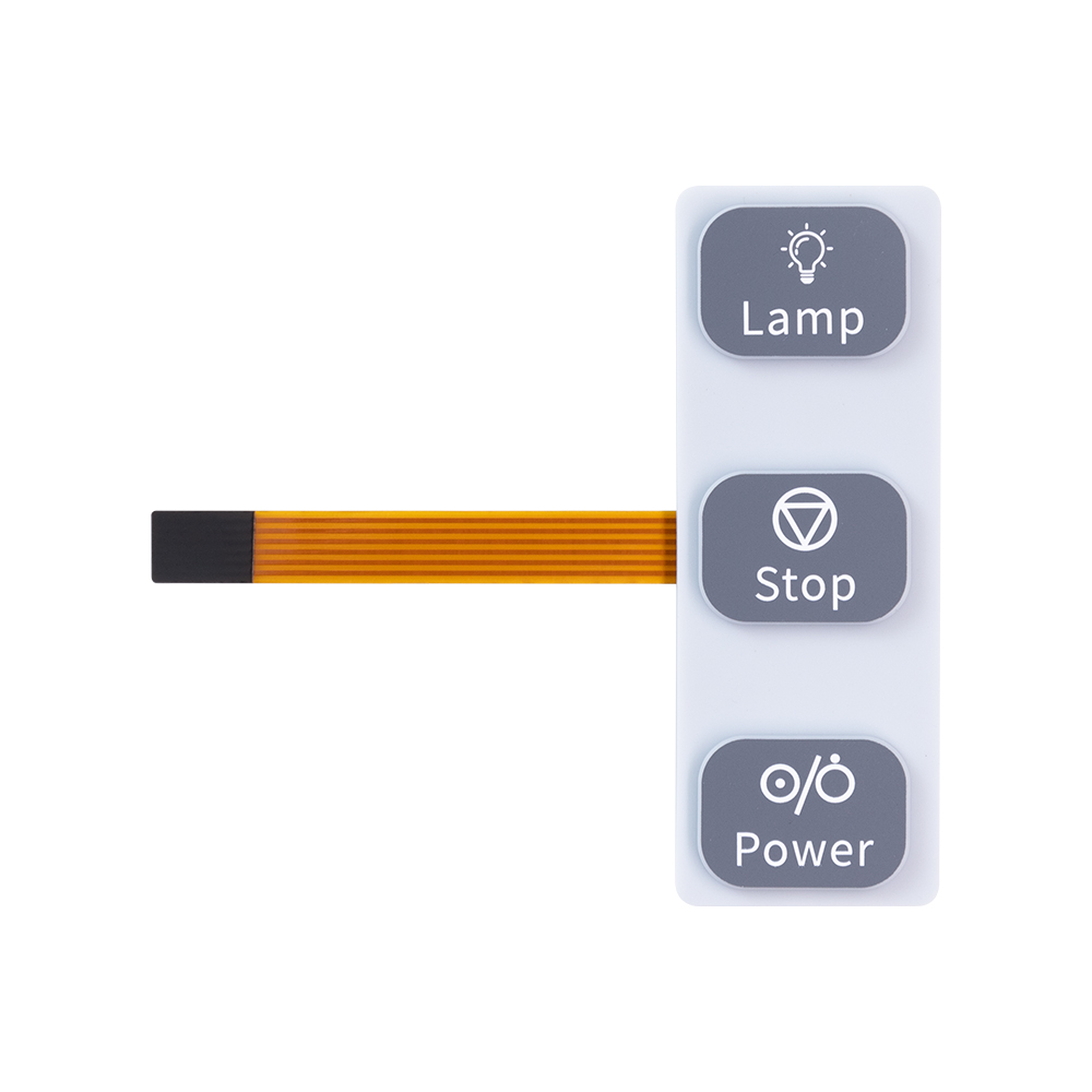
We provide rugged motor-drive PCBA solutions (utilizing BTS7960 high-current architectures and BLDC controller boards), matched with sealed IP65-rated tactile membrane keypads that resist industrial leather dust, lubricants, and continuous mechanical pounding over millions of cycles.
Heritage Conservation, Smart Museum IoT & Architectural Lighting
Florence’s world-renowned museums, such as the Uffizi Galleries and the Accademia, demand non-invasive, ultra-compact environmental logging systems (temperature, relative humidity, UV radiation) to safeguard irreplaceable Renaissance masterworks.
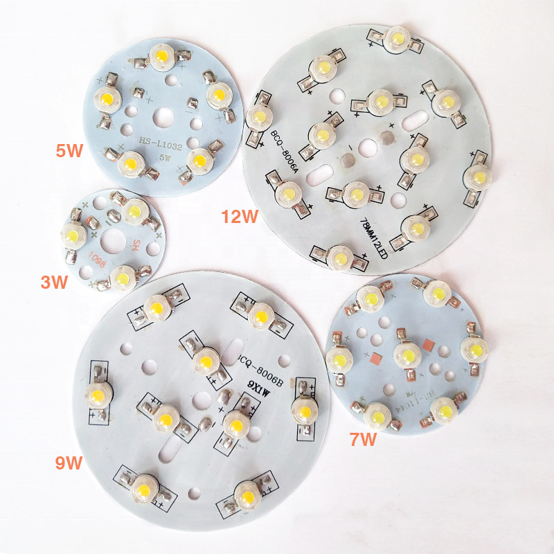
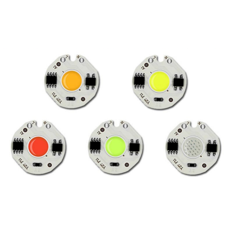
Our miniaturized Polyimide FPCs, driverless AC COB LED substrates, and low-power IoT PCBA platforms allow Tuscan restoration engineers to conceal micro-sensors and architectural exhibition luminaires inside historic architectural cornices without disturbing delicate structures.
State-of-the-Art PCB & PCBA Fabrication Parameters
Benchmark our manufacturing capabilities against IPC-A-600 (bare board acceptability) and IPC-A-610 (electronic assembly acceptability) standards.
| Technical Parameter | Standard Prototype Capability | Advanced Production Capability | Florence Regulatory/Application Alignment |
|---|---|---|---|
| Layer Count | 1 – 8 Layers | Up to 32 Layers (Rigid), 1-16L (FPC) | Multilayer compact computing & IoT sensors |
| Base Materials | FR-4 Standard (Tg 130-140°C) | High-Tg FR4 (Tg 170-180°C), Rogers, Polyimide, Al 5052/6061 | Resistant to automotive heat and lead-free reflow |
| Dielectric Thermal Conductivity | 1.0 W/m·K (Standard MCPCB) | 2.0 to 5.0 W/m·K (Ultra-high Thermal) | Photonic cooling and architectural floodlights |
| Min. Trace Width / Spacing | 0.1mm (4 mil) / 0.1mm (4 mil) | 0.065mm (2.5 mil) / 0.065mm (2.5 mil) | High density BGA routing and fine-pitch ICs |
| Min. Mechanical Drill Hole | 0.20 mm (8 mil) | 0.15 mm (Laser Microvia ≥ 0.075 mm) | HDI blind & buried via integration for wearables |
| Surface Finishes | HASL Lead-Free, OSP | ENIG (Electroless Ni / Immersion Au), ENEPIG, Hard Gold | RoHS 3 compliant, gold-contact oxidation prevention |
| SMT Placement Accuracy | ±0.035 mm (±35 μm) | ±0.02 mm (01005 passives, 0.3mm pitch BGA) | Diagnostic sensor front-ends, compact modules |
| Testing Protocols | 100% Flying Probe E-Test, AOI | X-Ray (BGA), Functional In-Circuit (ICT), FAI | Eliminates field failures in high-precision setups |
End-to-End Traceable Manufacturing Process Flow
Every board produced in our Shenzhen facility adheres to strict traceability standards before boarding air freight to Florence (FLR) or regional logistics centers.
DFM Engineering Audit
Within 24 hours of Gerber and BOM submission, our CAM team validates trace-to-copper clearances, hole-to-edge distances, and checks bill-of-materials lifecycle availability.
Laser Direct Imaging (LDI)
Precision optical imaging directly prints internal circuit architecture onto photosensitive dry films, preventing phototool expansion errors on multilayer stacks.
Automated Optical Inspection
High-resolution inner layer AOI systems cross-reference etched copper geometry against pristine CAD data, detecting microscopic shorts or pinholes prior to vacuum lamination.
Controlled Via Metallization
Electroless copper line deposition followed by electrolytic acid copper plating guarantees a minimum hole wall thickness of 20 to 25 μm (Class 2 / Class 3).
Liquid Photoimageable Mask
Automated spray coating applying high-temperature solder mask (Green, Matte Black, White for LED lighting) with exceptional dielectric strength and UL 94V-0 flammability ratings.
Surface Passivation
Deposition of Lead-Free HASL, ENIG, or Immersion Silver ensures superior coplanarity for fine-pitch SMT assembly while maintaining prolonged shelf-life under Mediterranean humidity.
Dual-Sided Flying Probe Testing
100% of bare boards undergo automated continuity and isolation checking at 250V to identify microscopic opens, trace leaks, or high-resistance vias.
Turnkey SMT, AOI & X-Ray
High-speed pick-and-place lines mount 01005 passives and BGAs with nitrogen reflow soldering, followed by 3D AOI and 2D/3D X-Ray void inspection below 10%.
Procurement Dynamics: How Tuscan OEMs Optimize Hardware Supply Chains
Emerging hardware trends reveal significant supply chain repositioning among Italian procurement directors seeking resilience against component obsolescence.
Consolidated BOM Turnkey Sourcing
Procurement officers in Florence frequently express fatigue managing separate vendors for bare PCBs, passives, semiconductors, custom keypads, and heat sinks. By partnering with a single turnkey manufacturer capable of managing component kitting and PCB fabrication simultaneously, lead times are compressed by up to 35%.
Legacy PCBA Cloning & Modernization
The textile and machinery sector in Prato and Florence often operates sophisticated legacy manufacturing equipment whose original PCB control boards are discontinued. Our engineering service specializes in non-destructive PCBA cloning, reverse engineering schematics, and migrating outdated DIP components to modern SMT alternatives.
Green Manufacturing & Decarbonization
With the European Green Deal and corporate ESG mandates becoming central to Italian enterprises, energy-efficient driverless LED modules, halogen-free laminates, and zero-effluent manufacturing processes provide Florence businesses with verifiable sustainability credentials.
Buyer FAQ: Sourcing PCBs & PCBA Directly from China to Florence
Clear, definitive answers to legal, fiscal, logistics, and engineering inquiries common among Italian hardware innovators.
What specific documentation is required to clear CE-compliant PCBs through Italian Customs (Dogana)?
Bare printed circuit boards are considered passive sub-assemblies and are generally classified under TARIC code 8534.00 (Printed Circuits). To facilitate seamless clearance through Italian customs (such as at Florence Peretola Airport, Bologna Interporto, or Milan Malpensa customs terminals), we provide:
- Commercial Invoice indicating complete description, net weight, and TARIC codes.
- Declaration of Conformity confirming compliance with RoHS 3 (Directive 2015/863/EU) and REACH (EC 1907/2006).
- UL Flammability Certification (UL 94V-0 file number marked visibly on the silkscreen).
- Certificate of Origin to assist with any preferential trade or duty audits.
For turnkey PCBA (classified under TARIC 8542 or 8543), full component traceability files are provided to support your Declaration of Conformity under the EU EMC Directive.
How does our company handle Italian VAT (IVA) and customs duties when importing from Shenzhen?
Registered Italian corporations possessing a valid Partita IVA and an active EORI number (Economic Operators Registration and Identification) can import seamlessly. Typical shipping terms are DAP (Delivered at Place) or DDP (Delivered Duty Paid via courier services like DHL, FedEx, UPS):
- Customs Duty: Bare PCBs under TARIC 8534.00 typically carry a 0% third-country duty rate into the EU.
- Import IVA (22%): Standard Italian VAT of 22% is assessed on the CIF value and cleared either through your forwarder's deferment account or reverse-charged if your company has registered as a regular exporter (plafond IVA).
What is the door-to-door transit timeframe from Shenzhen to Florence?
For express prototypes (urgent medical or laser optics design cycles), air express shipments (via DHL Express / FedEx Priority) take 3 to 5 business days from dispatch in Shenzhen to physical delivery at your facility in Florence, Scandicci, Calenzano, or Campi Bisenzio. For production batch orders over 200 kg, consolidated air freight to Bologna or Milan followed by bonded ground transport requires 7 to 10 days, optimizing freight costs significantly.
Can you manufacture aluminum LED boards to custom mechanical contours for historic architectural fittings?
Yes. Many historic restoration installations across Florence require circular, curved, or ultra-thin crescent-shaped aluminum MCPCBs to integrate into classical wall sconces and vault illumination channels. We utilize high-precision CNC V-scoring, automated milling routers, and punch tooling to achieve contour tolerances within ±0.1 mm, accommodating screw counterbores and cable cutouts without delaminating the aluminum-dielectric bond.
How do you verify genuine component provenance for turnkey PCBA assemblies?
We source 100% directly from verified Tier-1 authorized global distributors (including Arrow, Digi-Key, Mouser, Avnet) and direct chip manufacturer partnerships in Shenzhen and Hong Kong. Every sensitive semiconductor, microcontroller, or power MOSFET is inspected under magnification, date-code verified, moisture-baked according to J-STD-033, and backed by manufacturer CoCs (Certificates of Conformance). We never procure grey-market or refurbished components without client consent.
What is your Minimum Order Quantity (MOQ) for prototypes versus production?
We support agile hardware engineering with low minimums: prototype runs start from as low as 5 pieces for bare PCBs, flexible circuits, and turnkey PCBA. Once prototypes are verified and signed off by your engineering team, production effortlessly scales to thousands of panels per month with automatic panelization optimization to minimize scrap rate.
Why Florentine Hardware Leaders Entrust Their Builds to VUKO
Combining 14+ years of precision export experience, verified manufacturing facilities, and localized technical support.
Complimentary DFM Check
Every Gerber and BOM package undergoes rigorous automated and engineer-led Design for Manufacturability (DFM) verification prior to invoicing. We catch errors before they cost money.
Rapid Prototyping Speed
Standard double-sided FR-4 boards delivered in 24 to 48 hours; multilayer and aluminum boards in 3 to 5 days; turnkey PCBA in 10 to 15 days including global component procurement.
Financial Security
Protected under Alibaba Trade Assurance and standard European business credit terms. Payment is safeguarded from contract signature until successful physical delivery and verification.
Total Stack Solutions
Eliminate multiple purchase orders. We manufacture the bare board, source components, assemble SMT/DIP, provide IP65 membrane switches, and integrate thermal heat pipes under one roof.
Accelerate Your Florence Hardware Project Today
Whether you are developing clinical medical analyzers, precision laser electronics, automated luxury tooling, or high-efficiency LED luminaires, our engineering desk is ready to review your Gerber, BOM, and mechanical files.
Get a Quote