Featured Flexible Circuits, PCBA & HMI Assemblies
Comprehensive electronic interconnect systems, bare board flex fabrications, and electro-mechanical control modules ready for rapid prototyping and scale-up production.
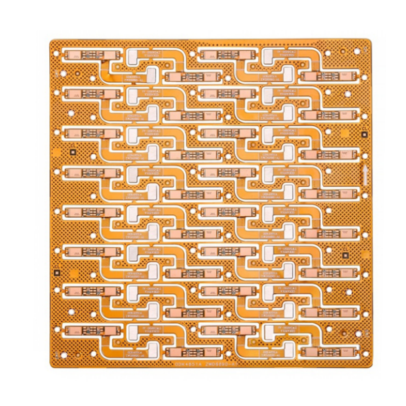
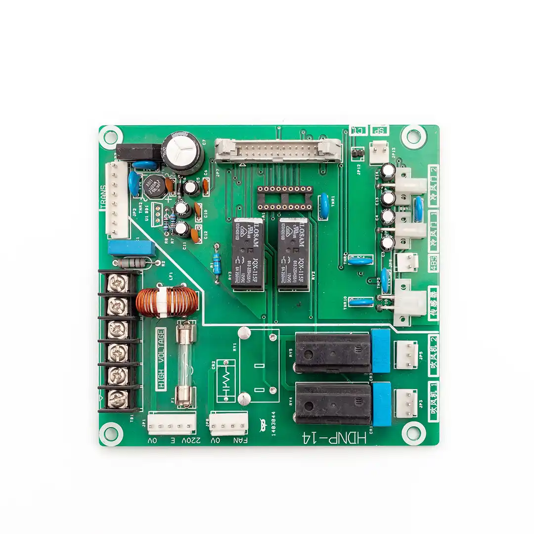
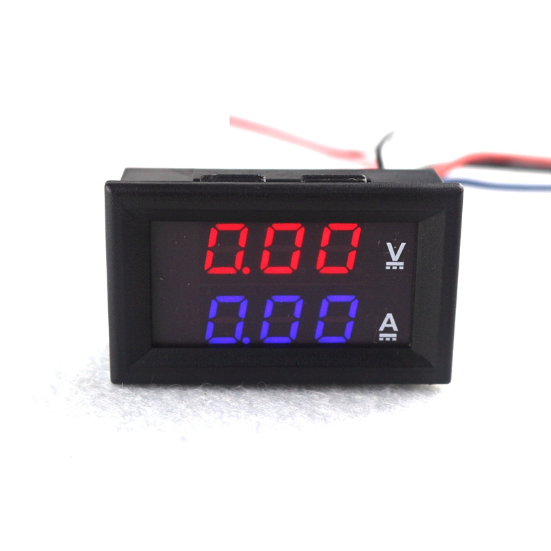
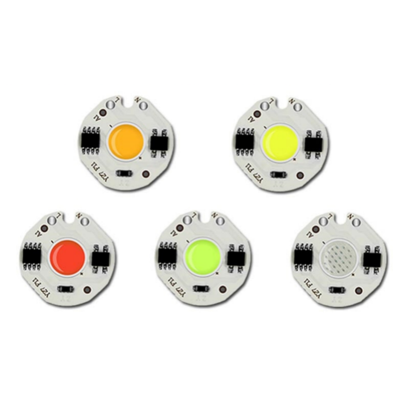
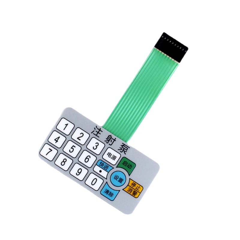
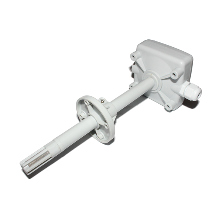
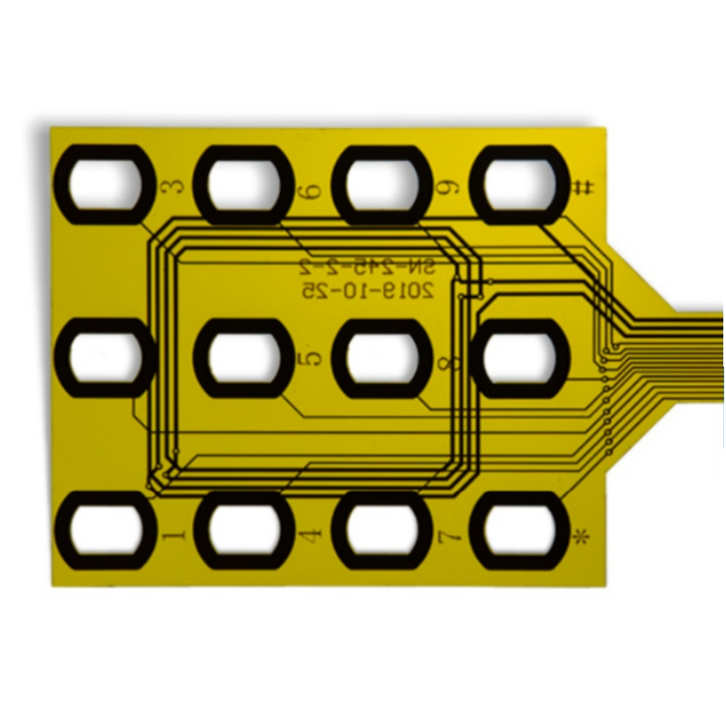
Single-Sided Flexible PCB Architecture & Substrate Physics
A rigorous examination of dielectrics, copper metallurgy, coverlays, and mechanical dynamics under IPC-6013 standards.
Single-sided flexible printed circuits (FPCs)—classified under IPC-6013 Type 1—form the bedrock of high-reliability, dynamic interconnect engineering. Unlike conventional FR4 rigid boards that exhibit inelastic brittle fracture under bending stress, single-sided flex circuits utilize a single conductive copper layer metallurgically bonded to a dielectric film base. For hardware engineers across Greater Philadelphia and the Mid-Atlantic industrial corridor designing ultra-thin medical probes, dynamic printer heads, surgical robotic end-effectors, or rugged naval telemetry arrays, understanding the interfacial physics of FPC substrate selection is critical to preventing premature trace fatigue and conductor cracking.
The core substrate typically consists of high-performance Polyimide (PI) film, predominantly DuPont Kapton® or equivalent poly(4,4'-oxydiphenylene-pyromellitimide) resins, ranging from 12.5 µm (0.5 mil) to 50 µm (2 mil) thicknesses. Compared to lower-cost Polyethylene Terephthalate (PET) films—which suffer thermal degradation above 105°C and cannot withstand conventional lead-free surface mount technology (SMT) reflow profiling—polyimide exhibits continuous operating thermal thresholds exceeding 200°C, dielectric strengths exceeding 200 kV/mm, and phenomenal dimensional stability across extreme humidity gradients.
Adhesiveless vs. Adhesive-Based PI
Adhesive-based laminates employ modified acrylic or epoxy resins to bond the copper foil to the polyimide base. While cost-effective for static bend-to-fit configurations, the adhesive layer introduces thermal expansion mismatch (higher z-axis CTE) and dampens high-frequency signal integrity. In contrast, our adhesiveless cast polyimide laminates bond copper directly to the film, yielding thinner overall stacks, superior dynamic flex life, and enhanced flame retardance meeting UL 94V-0 standards.
RA vs. ED Copper Metallurgy
For high-cycle dynamic flexing, Rolled Annealed (RA) Copper is mandatory. The continuous horizontal grain micro-structure formed through rolling mills allows the copper lattice to stretch and compress elastically, exceeding 1,000,000 flex cycles at tight radii. Conversely, Electro-Deposited (ED) Copper exhibits a vertical columnar crystal structure optimized for fine-pitch static traces but susceptible to micro-fracture during repeated movement.
Protective Coverlay Lamination
Traditional rigid solder mask inks crack under repeated flexing. Single-sided FPCs utilize a flexible polyimide coverlay (typically 0.5 mil to 1.0 mil PI coated with 1.0 mil thermosetting adhesive) vacuum-pressed under hydraulic lamination. This encapsulates the copper traces along the neutral mechanical axis, providing total galvanic isolation, chemical immunity, and moisture protection against environmental contaminants.
By keeping the copper conductor precisely aligned along the circuit's mechanical neutral axis—where neither compressive nor tensile forces dominate during bending—single-sided flexible PCBs achieve extraordinary bend radii down to 6x to 10x total finished thickness for dynamic applications, and up to 3x thickness for static installation folds. This mechanical resilience enables hardware teams to eliminate bulky wire harnesses, board-to-board connectors, and labor-intensive manual wiring assemblies.
Philadelphia & Delaware Valley Industrial Application Matrix
Targeted manufacturing solutions supporting Life Sciences, Defense, Process Automation, and Smart Infrastructure clusters across Southeastern Pennsylvania and South Jersey.
The Greater Philadelphia metropolitan region represents one of the United States' premier high-technology, healthcare, and advanced manufacturing epicenters. Anchored by the University City science corridor, the King of Prussia biopharma cluster, the Exton/Malvern medical alley, the Conshohocken industrial IoT corridors, and the Philadelphia Navy Yard defense enclave, regional hardware developers demand specialized electronic manufacturing capabilities that adhere to strict domestic regulatory frameworks while maintaining competitive global economics.
Cell & Gene Therapy Diagnostic Instruments
Philadelphia's status as "Cellicon Valley" drives constant innovation in automated bioreactors, flow cytometers, microfluidic cartridges, and portable blood analyzers. Single-sided FPCs are crucial for integrating miniaturized optical sensors and disposable biosensor electrodes where ultra-low mass, chemical biocompatibility, and high contact density in compact fluidic manifolds are paramount.
Philadelphia Navy Yard & Defense Telemetry
With naval architecture, unmanned marine systems, and ruggedized communication hardware engineered along the Delaware River waterfront, our custom polyimide FPCs replace heavy copper harnesses. They endure sustained shock, vibration, and salt-fog corrosion while delivering clean telemetry between high-density sonar heads and internal processing units.
HVAC Ducting & Environmental Automation
Mid-Atlantic industrial facilities rely on continuous environmental monitoring. As featured in our smart duct-type humidity and temperature sensor housings, single-sided flex tails allow sensors to be positioned deep inside high-velocity duct airflow without disrupting air distribution or suffering contact oxidation.
Driverless Architectural Solid-State Lighting
From modern high-rises in Center City Philadelphia to commercial industrial complexes in Montgomery and Bucks counties, our single-sided flexible LED circuits and driverless COB chip light engines provide continuous, uniform lumen output, fitting seamlessly into tight linear extrusions and curved architectural channels.
HMI & Sealed Medical Control Consoles
Hospitals, diagnostic suites, and food packaging lines across Southeastern PA require IP65/IP67 washdown-proof human-machine interfaces. By pairing single-sided flex circuits with waterproof tactile membrane switches and digital printing overlays, we supply hermetically sealed keypads resilient against harsh sterilization fluids.
Robotic Packaging & Warehouse Automation
With massive e-commerce fulfillment hubs expanding along the I-95 and PA Turnpike logistics corridors, robotic sorting arms and automated guided vehicles (AGVs) require dynamic flex cables capable of millions of torsional and continuous bend cycles without conductor degradation.
Modern PCB Sourcing Trends in the Greater Philadelphia Region
Balancing rapid prototyping agilities with high-volume cost containment through dependable offshore manufacturing channels.
Over the past five years, electronic procurement teams in Pennsylvania, New Jersey, and Delaware have shifted from fragmented, multi-tier vendor contracting to unified, turnkey manufacturing partnerships. As device complexity escalates while product design lifecycles compress from 18 months to under 24 weeks, hardware startups and tier-one OEM defense sub-contractors alike cannot afford the latency and finger-pointing caused by splitting bare-board fabrication, component sourcing, SMT assembly, and mechanical integration across disparate entities.
Key procurement and technical trends shaping the Philadelphia market include:
- Hybrid Agile Prototyping to Volume Scaling: Regional engineering centers frequently run initial 5-to-10-piece prototype builds for immediate mechanical fit and DFM validation before ramping smoothly into tens of thousands of production units. Shenzhen VUKO's low minimum order quantity (starting at 5 pieces) directly addresses this demand without penalizing engineering teams with punitive NRE (Non-Recurring Engineering) setups.
- Stringent Regulatory and Material Traceability: Medical and defense applications requiring FDA 510(k) clearances or MIL-STD qualification demand full material pedigree. Procurement teams require UL 94V-0 flammability certificates, certified RoHS and REACH compliance, and complete lot traceability across all active and passive electronic components.
- Direct Air Logistics into Philadelphia (PHL) and Newark (EWR): High-mix, quick-turn electronics shipments flow reliably through Philadelphia International Airport (PHL) cargo hubs and Newark Liberty (EWR) air terminals. By leveraging express customs clearance agreements and global courier networks (DHL, FedEx, UPS), lead times from factory inspection floor in Shenzhen to lab docks in King of Prussia or Camden average just 3 to 5 business days.
- Transition from Rigid Interconnects to Dynamic Flex: With industrial IoT edge sensors and wearable clinical monitors trending toward miniature ergonomic form factors, mechanical space constraints render standard rigid boards obsolete. Single-sided flex circuits offer a 70% weight reduction and an 80% volume decrease compared to conventional wiring, driving an aggressive substitution cycle across Mid-Atlantic engineering groups.
Precision Specifications & IPC-6013 DFM Benchmarks
Detailed technical thresholds for single-sided flexible PCB fabrication, stiffener integration, and SMT assembly.
| Design Parameter | Standard Capability | Advanced / Precision Limit | Engineering Notes |
|---|---|---|---|
| Base Polyimide Thickness | 25 µm (1.0 mil) | 12.5 µm (0.5 mil) or 50 µm (2.0 mil) | Dupont Kapton or adhesiveless equivalent resin |
| Copper Foil Type & Weight | 1/3 oz (12 µm), 1/2 oz (18 µm) RA Copper | 1 oz (35 µm), 2 oz (70 µm) RA / ED | Rolled Annealed (RA) recommended for dynamic bending |
| Minimum Trace Width / Spacing | 0.075 mm / 0.075 mm (3 / 3 mil) | 0.050 mm / 0.050 mm (2 / 2 mil) | Laser direct imaging (LDI) with optical vacuum etching |
| Minimum Dynamic Bend Radius | 8x to 10x Total Thickness | 6x Total Thickness (Single-Layer Adhesiveless) | Conductor aligned at the mechanical neutral bending axis |
| Coverlay Type & Thickness | 1.0 mil PI + 1.0 mil Modified Acrylic | 0.5 mil PI + 0.6 mil Epoxy / Laser Cut | Provides complete chemical isolation and UL 94V-0 rating |
| Surface Finishing Options | Immersion Gold (ENIG: 1-3 µ" Au / 120-200 µ" Ni) | Hard Gold (up to 30 µ" Au for edge fingers), Immersion Tin, OSP | ENIG standard for fine-pitch SMT and ZIF connector contacts |
| Stiffener Materials | FR4 (0.2–2.0mm), Polyimide (0.05–0.25mm) | Stainless Steel (0.1–0.5mm), Aluminum Plate | Bonded with thermal curing adhesive or 3M pressure-sensitive tape |
| SMT Component Density | 0201 passives, 0.4mm pitch QFN/IC | 01005 chips, BGA, ultra-fine flex soldering | Requires dedicated high-temperature carrier pallets |
| Dimensional Outline Tolerance | ±0.10 mm (CNC Routing) | ±0.05 mm (UV Laser Cutting / Optical Die Punch) | Complex outlines, relief radius slots, and tear-drop tabs |
To ensure high manufacturing yields, our engineering team enforces strict Design for Manufacturability (DFM) principles during pre-production Gerber RS-274X and ODB++ review. We automatically verify tear-drop reinforcements at all pad-to-trace transitions to eliminate stress concentrations, optimize radiused curved traces rather than sharp 90° corners to prevent copper micro-cracking during dynamic flex cycles, and ensure stiffener edges overlap coverlay margins by at least 0.5 mm to prevent localized shear failures.
Shenzhen VUKO Electronics: Factory Strengths & Infrastructure
Combining Shenzhen's unmatched electronic component supply chain density with world-class quality verification systems.
Alibaba.com Onsite-Verified Supplier
VUKO Electronics undergoes rigorous onsite operational and trade audits by independent international testing bodies through Alibaba.com. With over 14 years of sustained export track record across North America and Europe, buyers benefit from verified production floor capacities, authenticated trade history, and secure Trade Assurance payment protection.
Turnkey SMT & BOM Sourcing Ecosystem
Situated in the heart of Shenzhen, our procurement team sources directly from authorized silicon foundries and component distributors. We kit complete BOMs—including active ICs, passive 0201 passives, precision sensors, connectors, and heat management parts—while cross-referencing lead times and detecting obsolete parts before PCB assembly.
Multi-Tier Quality Assurance & Testing
Every single-sided flexible PCB and PCBA assembly undergoes 100% electrical continuity testing (flying probe or dedicated bed-of-nails fixture), Automated Optical Inspection (AOI) for trace defects and solder joint fillet integrity, solderability testing, thermal shock testing (-40°C to +125°C), and custom functional test verification per client schematics.
Holistic HMI & Module Integration
We do not just produce bare boards; our workshops engineer fully integrated human-machine interfaces (HMIs). We integrate tactile metal-dome membrane switches, graphic overlays, capacitive touch panels, silicone rubber keypads, and custom digital LED voltmeters into singular, ready-to-mount modules.
Rapid Prototype to Mass Production Agility
Whether you require a 5-piece sample batch for functional bench testing in a Philadelphia university research incubator or a containerized mass delivery for an industrial OEM line in Pennsylvania, our scalable production lines transition without friction or extended lead times.
Dedicated Engineering & 24h Response
Our sales and technical support teams provide fluent English communication tailored to North American working windows. Every file package submitted receives comprehensive DFM feedback and an itemized quotation within 24 hours.
Ready to Accelerate Your Philadelphia Hardware Program?
Submit your Gerber files (RS-274X/ODB++) and Bill of Materials for a comprehensive engineering DFM audit and custom quotation within 24 hours.
Frequently Asked Questions for Philadelphia Procurement Managers
Key insights on tariffs, logistics, material specs, testing, and design parameters for Mid-Atlantic hardware engineers.
What specific files and parameters are needed to quote a single-sided flexible PCB project?
To provide a definitive quotation and DFM assessment, we require your complete Gerber archive (RS-274X or ODB++ format) including conductor layers, solder mask/coverlay cutouts, drill files, outline and contour routing, and stiffener profile layers. Please specify desired base polyimide thickness (e.g., 25 µm), copper foil weight (e.g., 1/2 oz or 1 oz RA copper), stiffener materials (FR4, PI, or Stainless Steel), surface plating (such as ENIG or immersion tin), and total target quantities. If your project includes surface-mount assembly (PCBA), please attach a complete Bill of Materials (BOM) specifying manufacturer part numbers, pick-and-place centroid coordinates, and any specialized functional testing documentation.
How do you ensure dynamic flex fatigue resistance in high-cycle Philadelphia industrial applications?
Dynamic flex survival depends heavily on metallurgic selection and mechanical stack-up geometry. For dynamic flexing applications (such as automated warehouse sorting heads or robotic linkages), we mandate Rolled Annealed (RA) copper foils rather than standard electro-deposited (ED) copper. Additionally, we verify that your conductor traces are positioned exactly along the neutral mechanical axis using adhesiveless polyimide laminates. We recommend keeping trace corners radiused with gentle curves rather than 90-degree angles, prohibiting vias or surface-mount pads within the designated flex deformation zone, and applying flexible polyimide coverlays rather than brittle soldermasks.
What are the typical shipping options and transit lead times to Philadelphia (PHL) and the Mid-Atlantic area?
We work closely with global tier-one air express couriers (DHL, FedEx, UPS) to provide door-to-door expedited delivery from our Shenzhen production facilities directly to facilities throughout the Philadelphia metropolitan area, King of Prussia, Conshohocken, and South Jersey. Standard air transit typically takes 3 to 5 business days from final vacuum packaging. For large mass-production volumes, ocean freight can be arranged directly into East Coast ports (such as the Port of Philadelphia or Port of New York and New Jersey) with customs brokerage and duty clearing handled according to your specified Incoterms (DAP, DDP, or FOB).
How does VUKO Electronics manage component authenticity and counterfeit prevention for turnkey PCBA?
Our internal electronic component sourcing department maintains direct relationships with authorized component manufacturers and franchised global distributors (e.g., Arrow, DigiKey, Mouser, and authorized domestic tier-one suppliers). Every batch of incoming semiconductors, passives, and active ICs passes incoming quality control (IQC) verification, including micro-inspection for packaging integrity, date code validation, pin coplanarity, and counterfeit identification under high-magnification optical scopes. We provide full component traceability and material certificates for medical and industrial qualification files.
Can you integrate stiffeners and double-sided adhesives for ZIF connector mating?
Yes. The majority of single-sided flex circuits interface directly with motherboards via Zero Insertion Force (ZIF) or Low Insertion Force (LIF) connectors. We accurately laminate polyimide (PI) stiffeners at the contact finger region to reach the exact required thickness profile (commonly 0.30 mm ± 0.03 mm) demanded by standard Hirose, Molex, or JST ZIF receptacles. Additionally, we integrate high-temperature FR4 stiffeners beneath SMT component clusters to prevent solder joint shear during flexing, as well as pre-applied 3M adhesives (such as 3M 467MP, 468MP, or 9448A) for immediate chassis and enclosure bonding.
What is your minimum order quantity (MOQ) for custom flex PCB engineering?
Our MOQ starts at just 5 pieces for bare flexible PCBs, turnkey PCBA prototypes, and custom membrane switches. This low barrier allows hardware innovators, university laboratory research spinouts, and enterprise R&D engineering divisions across the Delaware Valley to thoroughly test form, fit, and electrical function before committing financial capital to commercial production runs.
How are client intellectual property and sensitive Gerber design files safeguarded?
We recognize the rigorous proprietary value of hardware IP, especially across Philadelphia's life science, medical device, and defense ecosystems. We routinely execute bilateral Non-Disclosure Agreements (NDAs) prior to file transfer. Our secure design servers are protected by encrypted firewalls, and production drawings are compartmentalized strictly on a need-to-know basis within our engineering and CAM stations.
Partner with a World-Class Flexible PCB Manufacturer
Gain a direct competitive edge through high-yield engineering, comprehensive DFM reviews, and dependable turnkey delivery directly to your facility.
Get Catalog