Featured High-Frequency & Interconnect Solutions
Engineered for mission-critical telecommunications, cloud compute acceleration, IoT edge nodes, and tactile human-machine interfaces.
High-Frequency Multilayer PCB Stack-Up & Signal Integrity Engineering
Overcoming Insertion Loss, Phase Jitter, and Dielectric Dispersion in Sub-6GHz and Millimeter-Wave Layouts for Austin Hardware Teams.
Understanding the High-Speed Dilemma in Central Texas Hardware Design
The Austin-Round Rock-San Marcos metropolitan area has rapidly matured beyond software to become one of the premier advanced semiconductor, computing infrastructure, and defense electronics centers in North America. When engineering prototypes for 5G cellular modems, autonomous vehicle radar arrays, or hyperscale data processing acceleration cards, standard FR-4 dielectric materials fail to perform reliably. The dissipation factor (Df) of generic epoxy systems (ranging between 0.015 and 0.020) induces catastrophic signal attenuation at multi-gigahertz frequencies, causing digital eye diagrams to collapse and RF transceivers to fall out of compliance.
As a specialized high frequency multilayer PCB manufacturer and exporter directly supporting Austin engineering groups, Shenzhen VUKO Electronics utilizes premium microwave composite laminates including Rogers (RO4350B, RO4003C, RO3003), Taconic (TLY/RF series), and high-speed low-loss Megtron 6/7. By mastering hybrid multilayer lamination—combining high-frequency PTFE/ceramic prepregs with conventional high-Tg FR4 cores—we give Austin hardware engineers the ability to maintain precise characteristic impedance (Z0) on outer microstrip traces while dramatically optimizing total board cost on inner power and low-speed digital control planes.
Comprehensive Fabrication Capability Matrix
Below are our certified production limits for high-frequency multilayer rigid, flexible, and metal-core circuit board fabrication, fully compliant with IPC Class 2 and Class 3 standards:
| Engineering Parameter | Standard Production Limit | Advanced / High-Frequency Capability |
|---|---|---|
| Layer Count | 1 – 12 Layers | Up to 32 Layers (Hybrid Stack-up) |
| Laminate Substrates | Standard FR4, High-Tg FR4 (Tg > 170°C) | Rogers 4350B, 4003C, Taconic, Megtron 6, Teflon/PTFE |
| Dielectric Tolerance (Dk/Er) | ± 5% | ± 1.5% (± 0.05 Dk accuracy) |
| Controlled Impedance (Single/Diff) | ± 10% (50Ω / 100Ω) | ± 5% (Precision TDR certified) |
| Minimum Trace / Spacing | 4 / 4 mil (0.1mm / 0.1mm) | 2.5 / 2.5 mil (0.065mm / 0.065mm) |
| Microvia Aspect Ratio & HDI | 1:1 (Mechanical Via 10:1) | Laser Staggered & Stacked Microvias (1+N+1 to 3+N+3) |
| Surface Finishes | HASL, Lead-Free HASL, OSP | ENIG (Immersion Gold), ENEPIG, Immersion Silver |
| Copper Weight | 0.5 oz – 2.0 oz | Up to 6.0 oz (Heavy Copper for Power Modules) |
Microstrip, Stripline, and Ground Plane Dissipation Controls
Signal degradation in high-speed traces stems not only from substrate dielectric loss but also from conductor loss amplified by surface copper roughness. Skin effect forces current to travel along the outer skin of the copper foil as frequencies push past 10 GHz. If standard electrodeposited (ED) copper is utilized, the physical tooth profile of the foil introduces substantial phase delay and attenuation. Shenzhen VUKO utilizes reverse-treated foil (RTF) and very low profile (VLP) copper foils with surface roughness (Rz) under 1.5 µm for high-frequency multilayer stack-ups intended for Austin defense and networking hardware.
Furthermore, backdrilling is routinely deployed to excise unused plated through-hole (PTH) via stubs. In serial backplanes and PCI-Express Gen 5/6 routing, an unremoved via stub functions as an open quarter-wavelength transmission line stub, creating deep signal nulls at harmonic frequencies. Our precision depth-controlled backdrilling ensures residual stubs measure less than 0.20 mm, preserving channel signal integrity and eliminating jitter across 28 Gbps+ SerDes lanes.
Localized Applications in Greater Austin, Texas
Custom-tailored circuit board architectures addressing the exact technical and operational demands of Central Texas engineering hubs.
Data Center & AI Accelerator Platforms
Central Texas hosts major hyperscale data centers and supercomputing research centers. Our 14- to 24-layer high-Tg Megtron and Rogers-hybrid backplanes deliver the thermal endurance and ultra-low insertion loss required by AI cluster switches, GPU compute blades, and PCIe Gen 5 expansion assemblies operating continuously in high-density rack enclosures.
Automotive ADAS & Electric Mobility
With the rapid rise of automotive innovation and gigafactories along the SH 130 corridor, Austin has become an epicenter for electric vehicle powertrains and autonomous vehicle sensor suites. We provide ceramic-filled hydrocarbon laminates for 77GHz mmWave automotive radar systems and thick copper aluminum-core PCBs for onboard charging and battery monitoring modules.
Commercial IoT & Industrial Energy Systems
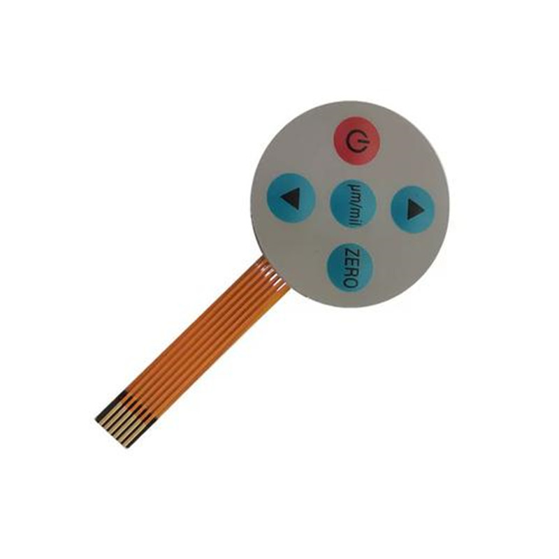
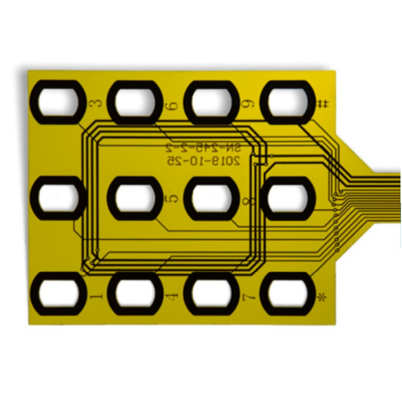
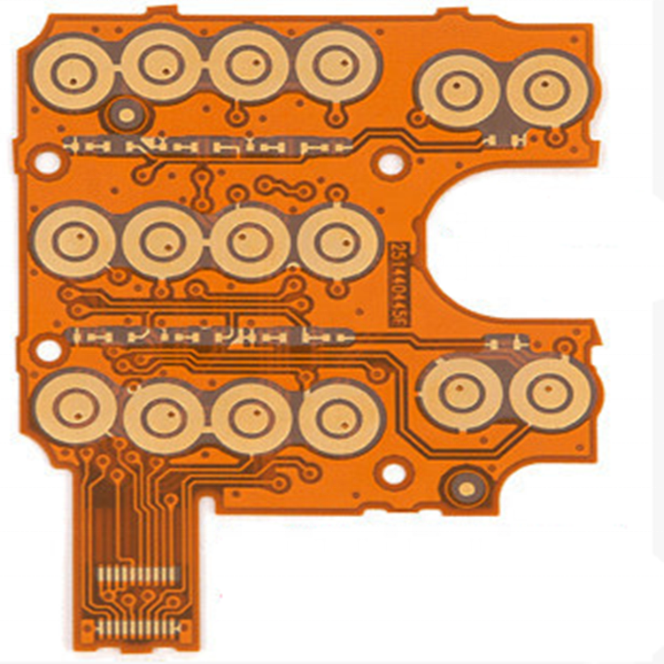
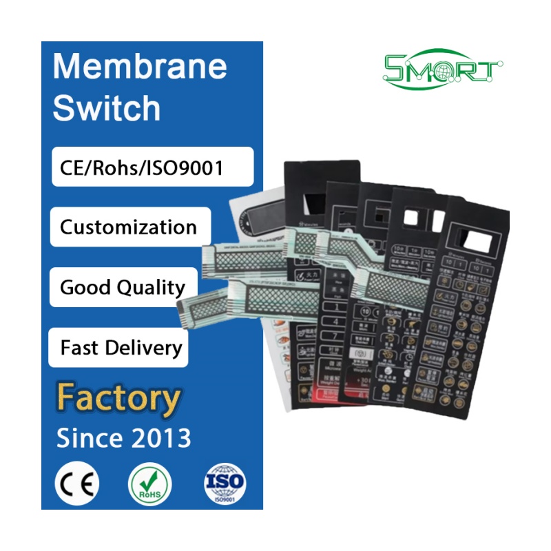
Austin energy tech startups and commercial IoT pioneers demand compact, low-profile flex circuits and waterproof membrane interfaces. Our FPC tails, flexible printed sensors, and IP65 tactile switch panels withstand harsh outdoor conditions, oilfield monitoring extremes, and municipal clean-grid monitoring environments throughout Texas.
Emerging Technology Trends in the Austin Electronics Sector
Strategic advancements reshaping PCB sourcing, rapid NPI iteration, and turnkey procurement for local engineering leads.
Rapid NPI to Volume Transition
Austin hardware incubators and enterprise skunkworks require prototype turnarounds in days, followed by instant scalability to hundreds of thousands of units without changing supplier engineering baselines.
Micro-BGA & HDI Integration
Next-generation system-on-chips (SoCs) and FPGA accelerators feature sub-0.4 mm ball pitch arrays, necessitating stacked microvias, via-in-pad plated over (VIPPO), and ultra-thin prepregs for dense escaping.
Supply Chain Resiliency & BOM Audits
Austin procurement managers increasingly hedge domestic assembly volatility by establishing direct offshore factory relationships in Shenzhen for verified BOM component sourcing and guaranteed wafer-level traceability.
Thermal Dissipation in Miniaturization
With edge devices packing immense RF amplification and compute power into sealed enclosures, hybrid metal-core and embedded copper coin techniques are replacing heavy external fans and extrusion heat sinks.
Why Austin OEM Hardware Teams Partner with Shenzhen VUKO
Combining Shenzhen's unmatched electronic manufacturing ecosystem with transparent, engineering-first customer communication.
Verified Supplier
Onsite-audited and verified manufacturing facility with 14+ years continuous international export history on Alibaba.com.
Zero-Defect Quality Control
100% flying probe testing, automated optical inspection (AOI), X-ray BGA verification, and comprehensive microsection reporting.
Pre-Manufacturing DFM Review
Dedicated RF and layout engineers review Gerber, drill, and netlist files within 24 hours to catch copper balance and stack-up flaws.
Flexible MOQ from 5 Pcs
Rapid low-volume NPI prototyping up to high-volume multi-thousand panel production, backed by Alibaba Trade Assurance.
Turnkey BOM & HMI Integration
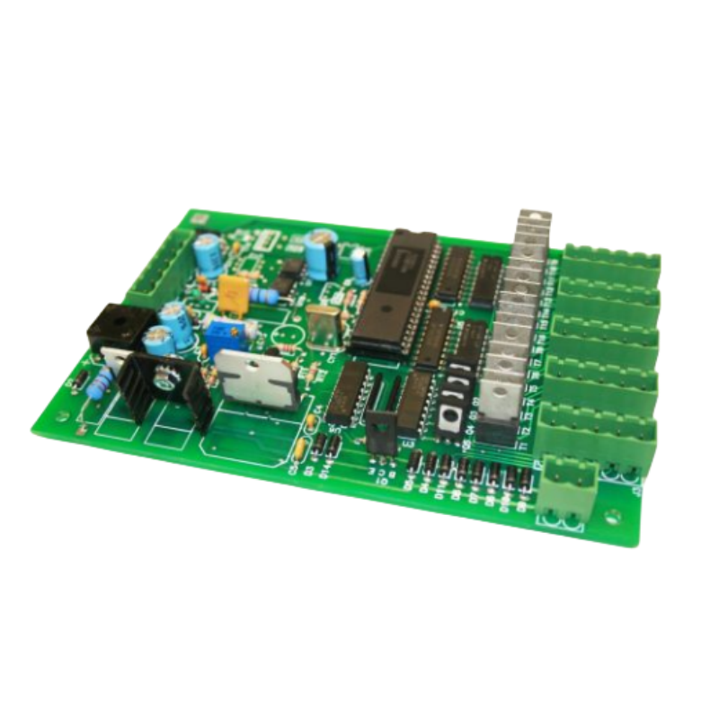
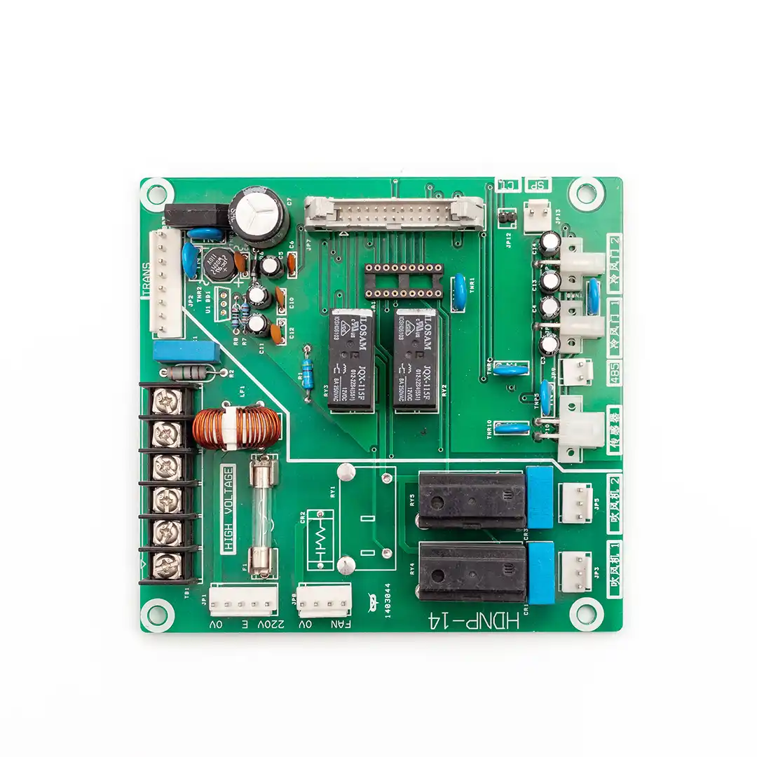
Consolidate bare boards, turnkey SMT/DIP placement, component procurement, custom FPC interconnects, and graphic membrane panels under one PO.
Austin Hardware Procurement FAQ
Direct answers to questions commonly raised by electrical engineers, sourcing leads, and hardware founders in Austin, TX.
What design files and specifications are required for an accurate high-frequency PCB quote?
For bare board fabrication, please upload Gerber files in RS-274X or ODB++ format along with NC drill files, IPC-356 netlists, and an explicit stack-up diagram specifying targeted core and prepreg dielectric constants (Dk/Df). Indicate copper foil weights, finished board thickness, surface finish (ENIG is strongly recommended for RF), and specific controlled impedance geometries (e.g., 50Ω single-ended microstrip, 100Ω differential pair). For turnkey PCBA, please also provide a structured BOM with complete manufacturer part numbers (MPN) and pick-and-place centroid files.
Can you manufacture hybrid multilayer stack-ups (e.g., Rogers combined with standard FR-4)?
Yes. Hybrid stack-ups represent one of our primary cost-optimization workflows for high-frequency hardware. We bond Rogers laminates (e.g., RO4350B or RO4003C) on layer 1 and layer 2 where high-frequency RF transmission lines run, while utilizing cost-effective high-Tg FR-4 (such as Shengyi S1000-2M or ITEQ IT-180A) for the internal power and ground distribution layers. Our engineering team calculates prepreg rheology and lamination press temperature profiles to guarantee zero delamination and reliable plated through-hole aspect ratios.
How do you verify controlled impedance before shipping boards to Austin?
Every controlled impedance panel incorporates test coupons fabricated on the outer margins that precisely mirror the geometry of your critical signal traces. We perform 100% Time Domain Reflectometry (TDR) testing across all coupons to verify impedance within ±5% (or ±10% based on your specification). A detailed microsection report displaying etched trace trapezoidal profiles, dielectric thickness, and TDR graphs is enclosed with your shipment paperwork.
What are your typical transit times and shipping channels to Austin, Texas?
All fabricated boards and assemblies are sealed in moisture-barrier anti-static packaging with desiccants and shipped directly via express air logistics (FedEx International Priority, DHL Express, or UPS Worldwide Saver). Transit time from our Shenzhen factory to your office or dock in Austin, Round Rock, or Cedar Park typically takes 3 to 5 business days, with full tracking and streamlined customs brokerage.
How does Alibaba Trade Assurance protect our transaction?
As an onsite-verified supplier on Alibaba.com for over 14 years, we offer complete buyer protection via Trade Assurance. Your initial payment remains secured in an escrow facility until you confirm receipt of boards that comply strictly with the approved Gerber package, IPC workmanship standards, and functional acceptance criteria agreed upon during order placement.