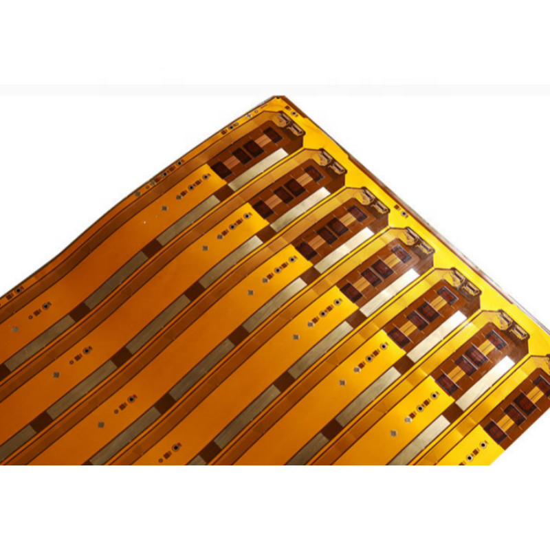
Engineered For Ultra-Compact Systems
Featured Engineering Hardware Portfolio
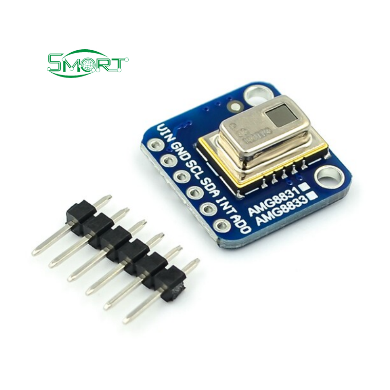
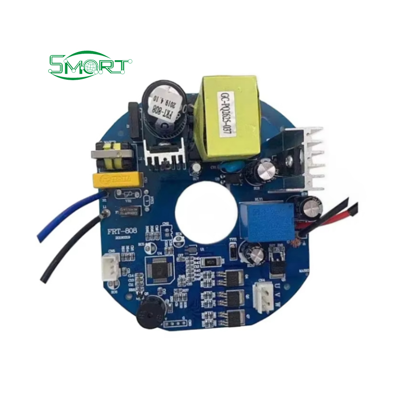
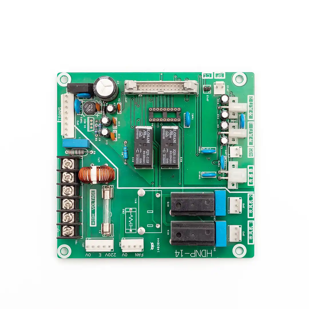
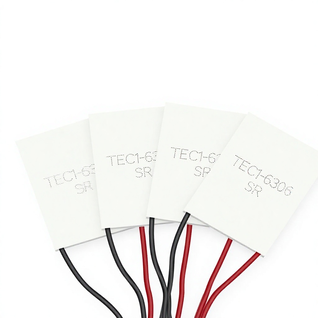
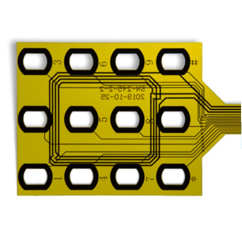
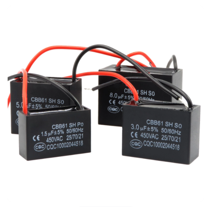
From single-board quick-turn FPC prototypes and dense multilayer rigid-flex matrices to complete turnkey SMT assemblies and thermal management modules.
Precision Regional Deployment
Multilayer Flex PCB Applications in the Balzers Industrial Sector
Situated at the heart of the Alpine Rhine Valley (Rheintal), Balzers is recognized globally for thin-film coating technology, high-vacuum measurement equipment, industrial automation, and optical sensor packaging.
High-Vacuum Instrumentation & Thin-Film Coating Systems
Balzers is synonymous with physical vapor deposition (PVD), plasma etching, and vacuum deposition apparatus. Multilayer flexible circuits manufactured with adhesiveless polyimide laminates eliminate outgassing risks under high-vacuum chambers (HV/UHV). Utilizing chemically etched RA copper foils, our 4-to-8 layer flexible interconnects route sensor channels and ion-gauge feeds through tight hermetic flanges without physical strain.
Sub-Miniature Optoelectronics & Photonic Transceivers
Precision optical instruments produced across Liechtenstein demand micro-pitch routing down to 0.05 mm (2 mil) trace and space. Our multilayer FPC boards integrate laser-microvias, blind/buried via topologies, and localized polyimide and stainless steel stiffeners, allowing direct flip-chip bonding and active alignment of photodiode arrays, optical transceivers, and laser diode emitters.
Industrial Motion Control & Dynamic Articulation
Robotic pick-and-place grippers and micro-positioning linear actuators manufactured in the Rhine Valley cluster experience millions of continuous flexural cycles. We provide custom flex designs engineered according to stringent IPC-2223 Class 3 standards, using rolled-annealed (RA) copper foils oriented longitudinally to ensure dynamic bending lifetimes exceeding 10,000,000 continuous cycles.
Multilayer Flexible PCB Technical Parameters for Balzers OEM Procurement
| Layer Count Range | 1 to 16 Layers (Rigid-Flex combinations up to 24 Layers) |
|---|---|
| Core Dielectric Materials | Adhesiveless Polyimide (DuPont Pyralux AP/LF, Panasonic Felios), PET for overlay circuits |
| Copper Foil Types | Rolled Annealed (RA) for dynamic flex applications; Electro-Deposited (ED) for static packaging |
| Dielectric Base Thickness | 12.5 µm (0.5 mil), 25 µm (1.0 mil), 50 µm (2.0 mil) |
| Minimum Trace / Space (L/S) | Outer: 0.05 mm / 0.05 mm (2 mil / 2 mil); Inner: 0.045 mm / 0.045 mm (1.8 mil / 1.8 mil) |
| Surface Finishes Available | Electroless Nickel Immersion Gold (ENIG), Immersion Tin, Immersion Silver, OSP, Hard Gold Fingers |
| Stiffener Technologies | Polyimide (PI), FR4 backing, Stainless Steel (SUS 304), Aluminum heatsink plates, 3M VHB bonding |
| Quality Standards & Flame Rating | IPC-6013 Class 2 & Class 3, IPC-A-610G Class 3, ISO 9001:2015, RoHS, REACH, UL 94V-0 |
Technological Evolution
Regional Trends Reshaping Flexible Electronics in Central Europe
How progressive industrial requirements across Liechtenstein, Switzerland, and Southern Germany are influencing flex PCB manufacturing architectures.
Shift Towards Adhesiveless Polyimide High-Tg Substrates
Due to higher operating temperatures in dense power electronics and vacuum sensors, Central European OEMs are shifting rapidly from adhesive-based substrates to adhesiveless polyimide films. Adhesiveless materials deliver superior dimensional stability (±0.05%), higher thermal decomposition temperatures (Td > 350°C), lower moisture absorption (< 0.8%), and remarkable dielectric constants (Dk 3.2 at 10 GHz) crucial for gigahertz signal transmissions.
Rigid-Flex Unification Over Cable Harness Assemblies
Cable harnesses and traditional multi-pin headers contribute to manual assembly errors, contact impedance instability, and unnecessary volume. In high-reliability automated inspection tools manufactured around Balzers, rigid-flex combinations are replacing cable assemblies. By consolidating multiple rigid PCBs into a single integrated flexible backbone, assembly labor drops by up to 60% while system vibration immunity is heightened exponentially.
Strict Traceability and Environmental Directives
Exporting machinery from Liechtenstein into the broader European Union requires compliance with EU RoHS 3 (Directive 2015/863/EU), REACH (EC 1907/2006), and the Conflict Minerals Regulation. Every multilayer flex circuit board we fabricate includes full lot traceability down to laminate batch numbers, copper foil certificates, and automated optical inspection (AOI) verification records.
Enterprise Strengths
Why Engineering Teams Partner with Shenzhen VUKO Electronics
Bridging Shenzhen's agile production acceleration with Central Europe's exacting engineering specifications.
14+
Years International Export Track Record
24h
Engineer-to-Engineer DFM Turnaround
100%
Flying Probe & AOI Electrical Verification
5 Pcs
Low MOQ for Advanced R&D Prototypes
Rigorous 12-Step Quality Control & IPC Compliance
From laser drilling of PTH vias, precision chemical electroless copper deposition, and dry film imaging, to flying probe electrical testing and automated vacuum packaging, every multilayer flex panel undergoes rigorous IPC-6013 Class 2/3 verification. Cross-sectional micro-section analysis ensures uniform plating thickness (≥20 µm in barrel walls) and flawless dielectric isolation.
Turnkey BOM Component Sourcing & Surface Mount Assembly
We provide complete turnkey procurement for active semiconductors, passive micro-components (down to 01005 / 0201 packages), ultra-fine pitch connectors, and custom functional modules. With high-speed Yamaha and Panasonic SMT pick-and-place lines, 3D SPI (Solder Paste Inspection), and nitrogen-purged reflow ovens, we assemble rigid, flexible, and aluminum boards with zero thermal deformation.
Holistic Human-Machine Interface (HMI) Integration
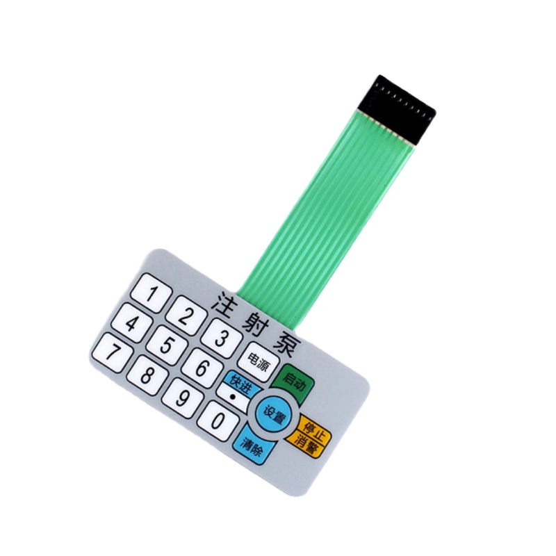
Beyond core circuit fabrication, VUKO produces custom waterproof tactile membrane switches, capacitive control panels, and silicone rubber keypads. This unified manufacturing scope enables industrial equipment builders in Balzers to source both internal interconnects and external operator panels from a single accountable manufacturer.
Procurement & Technical Queries
Frequently Asked Questions for Balzers & Swiss Border Buyers
Key details regarding customs clearance, DFM engineering verification, layer stack-up guidance, and rapid prototyping logistics.
How does VUKO manage customs clearance and shipping logistics into Balzers, Liechtenstein?
Liechtenstein participates in a customs union with Switzerland (Swiss VAT and customs regime apply). We supply full international commercial invoices, tariff HS codes (typically HS 8534.00 for bare PCBs and HS 8542.31 for assembled boards), and certificates of origin. Rapid air express via DHL, FedEx, or UPS Priority arrives directly at Swiss/Liechtenstein hubs within 3 to 5 business days with direct DDP or DAP options.
What specific engineering files are required for an accurate DFM review and quotation?
We require standard Gerber RS-274X or ODB++ fabrication data, NC drill files, and a comprehensive fabrication drawing specifying copper weight (0.5 oz, 1 oz, 2 oz), coverlay type, stiffener dimensions (FR4, PI, or stainless steel), and surface finish. For PCBA orders, please provide the bill of materials (BOM) with manufacturer part numbers (MPNs) and pick-and-place centroid coordinates (X-Y data).
Can you manufacture dynamic flex circuits that withstand millions of bending cycles?
Yes. Dynamic flex circuits must be engineered specifically to prevent copper fatigue. We utilize Rolled-Annealed (RA) copper foil rather than Electro-Deposited (ED) foil, ensure trace paths run perpendicular to the bend axis, employ staggered traces on adjacent layers to eliminate neutral axis stress concentrations, and enforce minimum bend radius rules (typically ≥ 10x board thickness for multilayer configurations).
What are your prototyping MOQs and typical lead times for multilayer flex boards?
Our prototype MOQ starts from just 5 pieces to support engineering research and early-stage product trials. Bare flexible PCB prototypes are routinely turned around in 5 to 7 working days, while rigid-flex prototypes and assembled turnkey boards typically require 10 to 15 working days depending on component availability.