Multilayer PCB Manufacturer & Supplier for Melbourne
Precision Engineering, Controlled Impedance, Quick-Turn Prototyping & High-Reliability PCBA for Victoria’s Tech Sector
Engineered Electronics & Interconnect Solutions
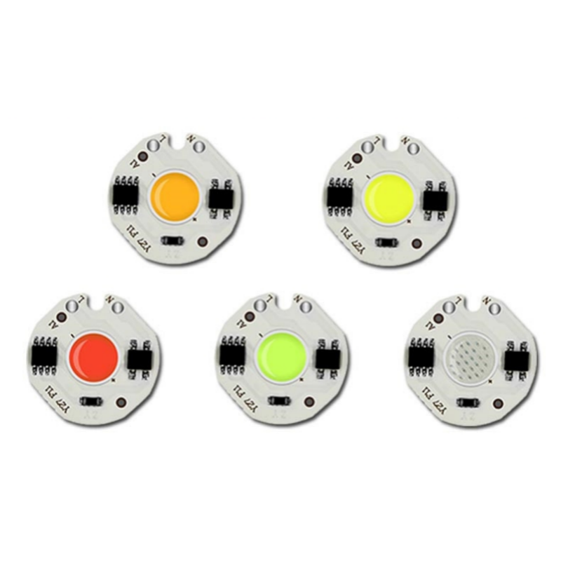
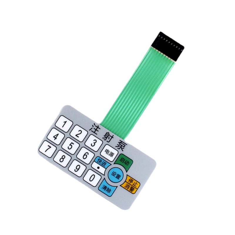
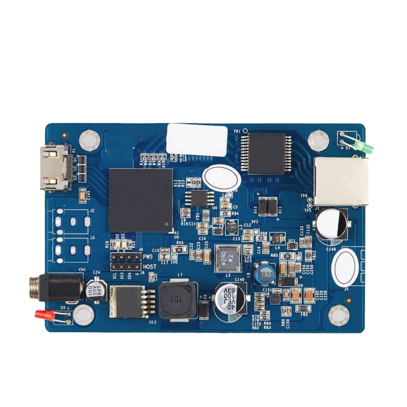
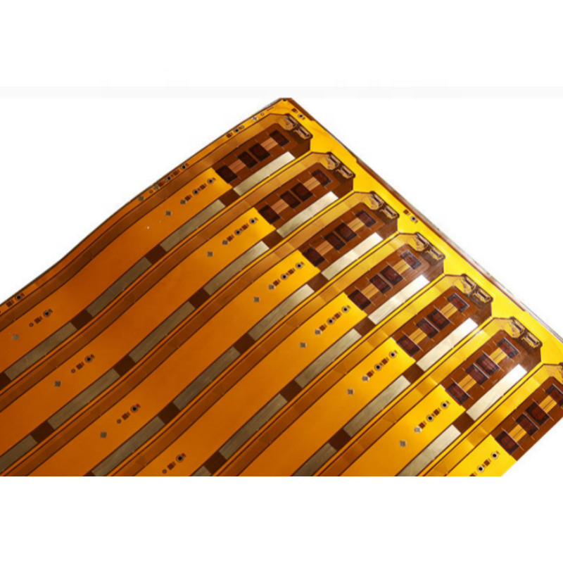
Precision bare printed circuit boards, high-density flexible interconnects, thermal management solutions, and human-machine interface assemblies for turnkey device integration.
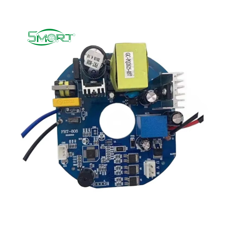
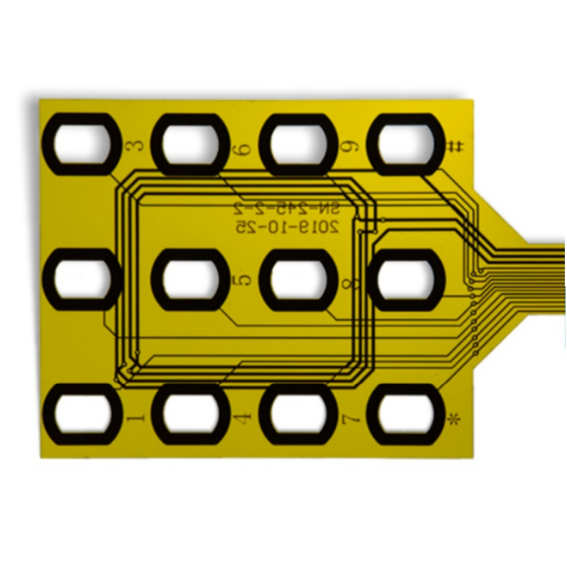
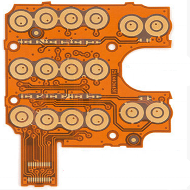
14+
Years Industry Export Experience
24h
DFM Engineering Review Turnaround
1-16
Multilayer Rigid & Flex Layer Capacity
100%
AOI & Flying Probe Electrical Testing
Engineering Multilayer PCBs for Melbourne's Advanced Tech Ecosystem
Melbourne has rapidly evolved into Australia’s primary epicenter for hardware technology innovation, medical diagnostic manufacturing, agritech telemetry, and green energy power conversion. From the biomedical research clusters in Parkville and Clayton to industrial automation specialists across Dandenong and Campbellfield, electronics designers in Victoria face rigid environmental, regulatory, and spatial constraints. Designing multilayer printed circuit boards (PCBs) for these mission-critical sectors requires significantly more than basic Gerber plotting; it demands rigorous material characterization, meticulous controlled impedance matching, optimized thermal via topologies, and uncompromising surface chemistry integrity.
Shenzhen VUKO Electronics delivers end-to-end multilayer PCB manufacturing, component kitting, and SMT assembly tailored explicitly to the needs of Melbourne-based original equipment manufacturers (OEMs), engineering consultancies, and hardware start-ups. Bridging early-stage prototyping with scalable medium-to-high volume production, we combine Shenzhen’s agile electronics manufacturing infrastructure with international traceability standards (ISO 9001, UL 94V-0, and IPC-A-600/610 Class 2 & Class 3).
Advanced Multilayer PCB Technical Capabilities
Modern multilayer stacks must manage high-speed differential signal routing, power plane decoupling, and thermal loads within constrained form factors. Below are the standard manufacturing tolerances and capabilities supported by our fabrication facilities:
Base Laminates & Stacks
- FR4 Standard / Mid-Tg: Tg 135°C–150°C
- High-Tg FR4: Tg 170°C–180°C (Shengyi S1000-2, IT-180A)
- Halogen-Free: RoHS compliant green substrates
- Metal Core (MCPCB): 1.0 to 5.0 W/m·K Aluminum/Copper
- Polyimide (PI): Flexible & rigid-flex substrates
Etching & Trace Tolerances
- Min. Trace Width / Space: 3.0 mil / 3.0 mil (0.075mm)
- Finished Copper Thickness: 0.5 oz to 6.0 oz
- Impedance Control: Single-ended & differential (±10% or ±5%)
- Outer Layer Copper Balance: Automated thieving inclusion
- Panel Thickness: 0.20 mm to 4.00 mm
Microvias & Mechanical Drilling
- Min. Mechanical Drill Hole: 0.15 mm (6 mil)
- Laser Microvia (HDI): 0.10 mm (4 mil) blind/buried
- Aspect Ratio: Up to 10:1 mechanical drilling
- Hole Wall Copper: 20µm minimum (IPC Class 2), 25µm (Class 3)
- Via Filling: Non-conductive epoxy plug & planarization (IPC-4761 Type VII)
Substrate & Surface Finish Selection for Victorian Operating Environments
Selecting the optimal surface finish is critical to preventing galvanic corrosion, ensuring long-term solder joint fatigue resistance, and maintaining signal integrity in variable ambient conditions—ranging from coastal marine installations along Port Phillip Bay to harsh dry inland mining or agricultural environments.
| Surface Finish | Thickness Specification | Shelf Life | Ideal Application in Melbourne Industry | IPC Class / Regulatory |
|---|---|---|---|---|
| Electroless Nickel Immersion Gold (ENIG) | Ni: 3-5 µm, Au: 0.05-0.1 µm (2-4 µin) | 12–24 Months | Fine-pitch BGA, medical instrumentation, precision RF sensors | IPC-4552 / RoHS Compliant |
| Lead-Free HASL (Sn/Ag/Cu) | 1.0–40 µm (variable profile) | 12 Months | Rugged industrial power distribution, lighting, cost-sensitive controllers | IPC-6012 / RoHS Compliant |
| Immersion Silver (IAg) | 0.15–0.40 µm | 6–12 Months | High-frequency 5G/IoT telemetry, low-loss RF interconnects | IPC-4553 / RoHS Compliant |
| Organic Solderability Preservative (OSP) | 0.20–0.50 µm | 6 Months | High-volume automotive sub-assemblies, basic consumer electronics | IPC-4555 / RoHS Compliant |
| Hard Gold Plating (Edge Fingers) | Au: up to 1.25 µm (50 µin) over Ni | >36 Months | PCIe connectors, repeated backplane insertion cards, test fixtures | MIL-G-45204 / IPC-6012 |
Localized Application Scenarios in Melbourne & Greater Victoria
The manufacturing demands of Victorian engineering hubs require high customization, rapid prototyping cycles, and seamless transitions into batch production. VUKO Electronics supports diverse local industry verticals:
1. Medical Diagnostic & MedTech Hardware
Victoria accounts for over 40% of Australia's biomedical research. We manufacture high-density 6-to-12 layer rigid-flex boards and ENIG multi-layer PCBs for wearable diagnostic monitors, infusion pump logic controllers, and point-of-care analytical devices, ensuring zero-defect soldering, low outgassing, and biocompatibility support.
2. Heavy Industrial & Agritech Telemetry
Deployments in regional Victoria require extreme durability against temperature cycling and vibration. Our 2-to-8 layer heavy copper boards (2–4 oz) and conformal-coated assemblies power robust tractor guidance systems, environmental water sensor nodes, and smart irrigation controllers.
3. Smart EV Charging & Renewable Microgrids
With Victoria's accelerating renewable investments, power density is paramount. We produce metal-core and hybrid aluminum-FR4 multilayer boards engineered to withstand high voltage transients, optimize junction cooling in DC-DC converters, and control smart EV charging wallboxes.
Technological Shifts Shaping Victorian PCB Procurement
Electronics engineering in Melbourne is currently experiencing three distinct shifts. First, the miniaturization of commercial IoT devices has dramatically accelerated the demand for Rigid-Flex and HDI (High-Density Interconnect) circuit topologies. By consolidating multiple rigid boards and ribbon cables into an integrated rigid-flex circuit, hardware teams eliminate mechanical connectors, substantially reducing board footprint, assembly labor, and point-of-failure risks.
Second, the local shortage of rapid electronic component sourcing has made turnkey PCBA services essential. Engineers can no longer afford to manage separate vendor pipelines for bare PCB fabrication, passive component buying from local distributors, and local assembly houses. VUKO Electronics’ factory-direct turnkey model handles PCB production, authorized component kitting (via direct relationships with original silicon manufacturers), and SMT/DIP placement under one roof in Shenzhen, delivering finished, tested assemblies straight to Melbourne doorsteps in as fast as 7 to 10 working days.
Why Melbourne Hardware Engineers Partner With VUKO Electronics
With over 14 years of verified manufacturing and export history, Shenzhen VUKO Electronics provides an enterprise-level bridge between early engineering ideation and mass fabrication. Our advantages directly mitigate international supply chain friction:
Pre-Production DFM Checks
Every Gerber package, IPC-2581 file, or BOM uploaded is reviewed by our Senior CAM Engineers within 24 hours. We identify acid traps, acute trace angles, inadequate solder dams, and component footprint mismatches before physical fabrication begins.
Full Turnkey Component Sourcing
Located within the heart of the Shenzhen electronics ecosystem, our component procurement team secures authentic, factory-direct ICs, passives, and active silicon. We provide lifecycle risk analyses, identifying end-of-life (EOL) or obsolete parts with verified drop-in alternatives.
Comprehensive Quality Inspection
Quality is backed by multi-stage test protocols: Automated Optical Inspection (AOI) for trace accuracy, 100% Flying Probe or Bed-of-Nails electrical testing, X-Ray inspection for leadless BGA/QFN solder voiding, and functional jig testing prior to vacuum packaging.
Frequently Asked Questions: Procuring PCBs from Melbourne
Key technical, logistic, and commercial questions answered for Australian engineering and procurement managers:
What specific manufacturing files do you require for a full turnkey PCBA quotation?
To deliver a comprehensive DFM analysis and quotation within 24 hours, please supply: 1) Gerber files in RS-274X format or ODB++ (including drill files, copper layers, solder mask, and silkscreen); 2) A complete Bill of Materials (BOM) in Excel format with clear Manufacturer Part Numbers (MPN), descriptions, designators, and approved alternative brands; 3) Pick-and-Place (centroid/XY data) for automated SMT lines; and 4) Any specialized schematic testing guidelines or programming hex files.
How fast can prototype orders be delivered to Melbourne or Victoria addresses?
Quick-turn bare multilayer PCB prototypes (2 to 4 layers) can be fabricated in 48 to 72 hours. Turnkey PCBA prototypes generally require 10 to 14 working days, depending on component availability. We partner directly with DHL Express, FedEx Priority, and UPS Express, ensuring door-to-door transit times from Shenzhen to Tullamarine Airport (Melbourne) of 3 to 5 business days.
How do you handle Australian regulatory compliance such as RoHS, UL, and RCM?
All laminates (Shengyi, ITEQ, Ventec), solder alloys (SAC305 lead-free), and surface chemistry comply with EU RoHS and REACH regulations, directly meeting Australia’s environmental standards. Our boards carry UL 94V-0 flammability ratings. For finished sub-assemblies requiring RCM (Regulatory Compliance Mark) compliance, we maintain precise component traceability to assist your lab certifications.
Do you accommodate low Minimum Order Quantities (MOQ) for Melbourne R&D projects?
Yes. We understand that local startups and university engineering teams need low-volume agility. Our MOQ starts at just 5 pieces for bare prototypes and assembled PCBAs. We support engineering iterations seamlessly from small verification runs up to high-volume commercial production without requalification delays.
Can you execute impedance control for high-speed differential pairs (USB 3.0, PCIe, DDR)?
Absolutely. We achieve ±10% (and down to ±5% on specialized request) controlled impedance tolerances. When submitting your design, specify the target single-ended (e.g., 50Ω) or differential impedance (e.g., 90Ω, 100Ω), target layer, and trace geometry. We calculate exact prepreg and dielectric core stack-ups using polar impedance modeling software and supply TDR (Time Domain Reflectometry) test coupons with your batch.
How are my payment and intellectual property rights safeguarded?
We routinely sign Non-Disclosure Agreements (NDAs) with Australian design teams to protect design schematics and firmware. Commercial payments can be safely processed via Alibaba Trade Assurance, providing payment escrow and order fulfillment protection, or through international wire transfer (T/T), PayPal, and Western Union.