Enterprise Product Portfolio
Precision High-Mix PCB, FPC & Assembly Solutions
Engineered to bridge agile Silicon Valley R&D with scalable, production-ready Asian electronics manufacturing. Every unit adheres to UL 94V-0, ISO 9001, and comprehensive DFM design rules.

Strategic Whitepaper
Navigating High-Mix, Quick-Turn Electronics Procurement in Santa Clara County
In the heart of Silicon Valley, electronic product developers in Santa Clara, Sunnyvale, Cupertino, and North San Jose operate under aggressive design sprints. Hardware startups and tier-one technology enterprises alike require prototype turnarounds within 24 to 72 hours, without sacrificing the stringent quality benchmarks dictated by IPC Class 2 and Class 3 manufacturing standards. The core challenge facing Santa Clara hardware architects is the notorious "prototype-to-production chasm"—where low-volume domestic prototype shops lack the economical infrastructure to scale, while high-volume overseas fabricators resist orders beneath exorbitant MOQs.
Shenzhen VUKO Electronics Co., Ltd. eliminates this logistical bottleneck. By establishing a direct cross-Pacific engineering pipeline, we provide Santa Clara purchasing and engineering teams with low-MOQ flexibility (from 5 pieces), comprehensive DFM (Design for Manufacturability) analysis, automated SMT lines, and direct turnkey BOM sourcing from Huaqiangbei's world-class supply nexus. We bridge prototype iterations directly into mass production runs, saving Silicon Valley OEMs up to 40% on engineering cycles and bill-of-materials overhead.
24h
DFM & Quote Response
Dedicated engineering reviews across PST and HKT operational windows.
5 pcs
Minimum Order Volume
Zero barrier to entry for proof-of-concept and agile test bed fabrication.
100%
Inspection & Verification
Standard flying probe, AOI, X-ray inspection, and dedicated functional testing.
14+
Years Global Exporting
Verified Alibaba Gold Supplier with Trade Assurance financial escrow.
Silicon Valley Deployment
Mission-Critical PCB Applications across Local Tech Sectors
From hyper-scale server architecture in Santa Clara data centers to autonomous mobility sensor stacks, our circuit boards and custom assemblies power Silicon Valley's foundational hardware stacks.
AI Cloud Data Centers & High-Speed Computing
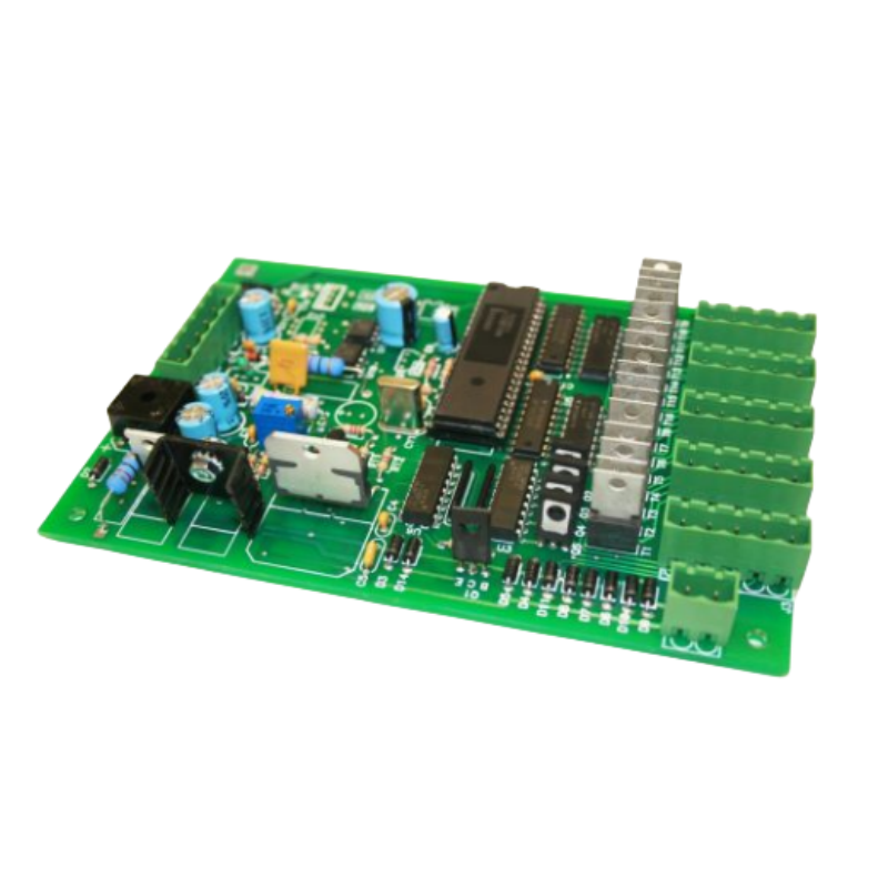
Santa Clara serves as the world capital for AI accelerator architecture. Our High-TG (TG170–TG180), low-loss PTFE/Rogers and High-Density Interconnect (HDI) multilayer bare boards feature controlled impedance tolerances within ±5%, micro-vias, and buried/blind via structures engineered specifically for 112G PAM4 signaling and rack-mount server acceleration.
Autonomous Mobility, LiDAR & Robotics
Silicon Valley autonomous vehicle teams in Palo Alto and Sunnyvale rely on our ruggedized rigid-flex and polyimide FPC circuits to interconnect high-resolution optical cameras, mmWave radar units, and solid-state LiDAR sensors within ultra-compact spatial envelopes, providing continuous vibration immunity and thermal resilience.
MedTech Diagnostic Systems & Bio-Instrumentation
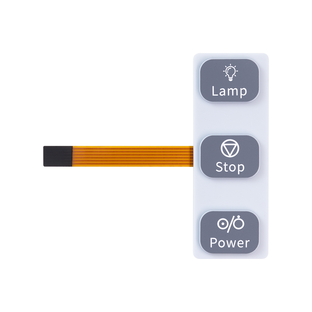
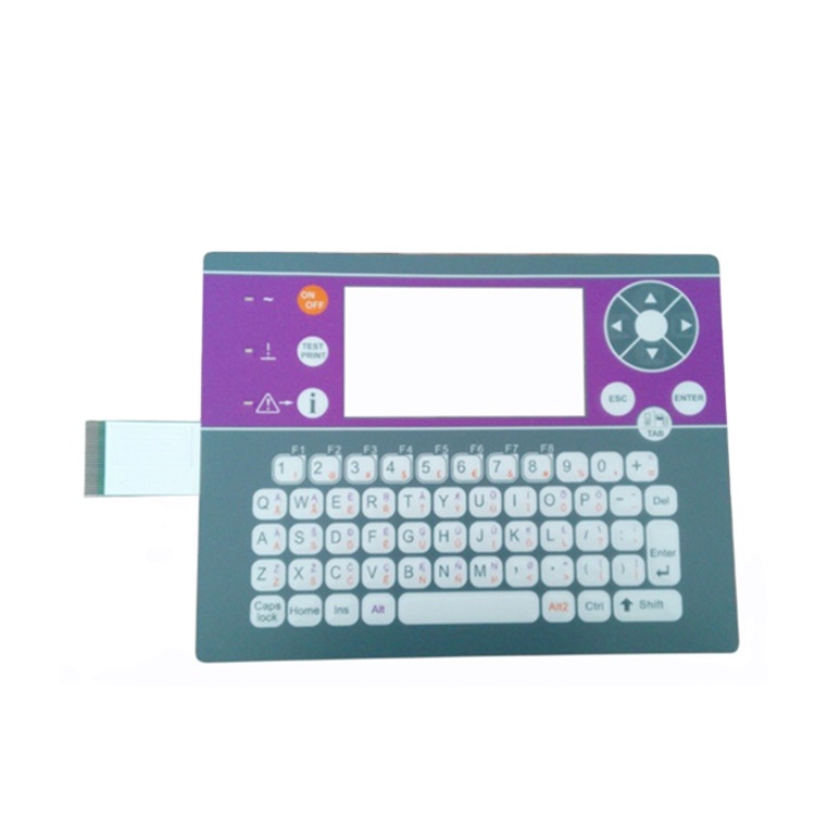
South Bay biomedical innovators demand uncompromising signal cleanliness and bio-compatible interfaces. We assemble precision SMT medical motherboards paired with sealed IP67 tactile membrane switches, incorporating anti-microbial overlays and gold-plated contacts resilient to chemical washdowns and autoclave sanitation protocols.
Industry Forecast
Key Hardware Manufacturing Shifts in Northern California
Market dynamics influencing how Silicon Valley engineering leads evaluate PCB, FPC, and turnkey assembly vendors in 2025 and beyond.
Trend 01 · Signal & Heat
Convergence of High-Power Density & Thermal Dissipation
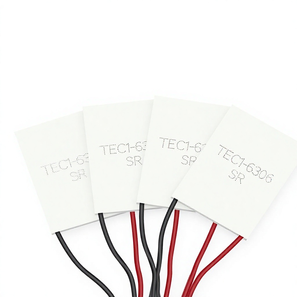
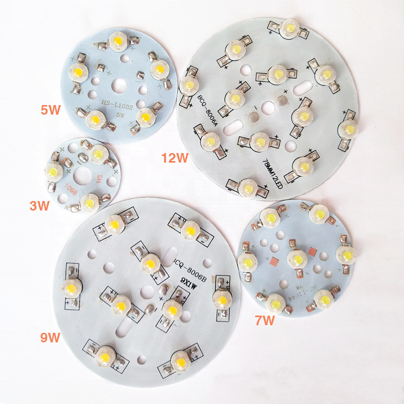
With edge AI devices and GaN/SiC power converters concentrating up to 100W/cm² of thermal load, conventional FR4 substrate configurations are obsolete. Santa Clara hardware architects increasingly specify custom MCPCB (Aluminum Core) with 2.0 to 5.0 W/m·K thermal conductivity dielectrics and hybrid copper-core sandwich panels integrated directly into Peltier TEC coolers to eliminate thermal throttling.
Trend 02 · Miniaturization
Rigid-Flex Eliminating Discrete Wiring Harnesses
Wearable neuro-tech headsets, handheld industrial diagnostic tablets, and compact aerospace drones designed in the San Jose metropolitan area are phasing out bulky pin-and-socket cable assemblies. Designers are consolidating entire subsystem interconnects into single multilayer Rigid-Flex architectures, lowering total weight while dramatically reducing RF signal loss.
Trend 03 · Resilient Sourcing
Turnkey Sourcing with Pre-Emptive Lifecycle Engineering
Prolonged component lead times and sudden active-IC obsolescence continue to disrupt Silicon Valley production rollouts. Engineering leaders now require offshore contract manufacturers who offer active BOM scrubs—identifying pin-compatible alternates, second-source passives, and active silicon allocations prior to committing to production stencils.
Engineering Superiority
Why Silicon Valley Hardware Teams Partner with VUKO
Headquartered in Shenzhen's cutting-edge manufacturing corridor, VUKO combines direct fab ownership with verified global export credentials, delivering seamless continuity from initial sample to volume container shipment.
Pre-Fab DFM Scrubbing
Every Gerber and ODB++ dataset is scrutinized by our senior CAM engineers within 24 hours, uncovering annular ring violations, trace clearances, and copper balancing hazards before tooling.
Rapid SMT Prototyping
Agile surface-mount assembly from 5 pieces. Dedicated prototype lines equipped for 01005 passives, 0.35mm pitch BGAs, and dual-sided high-density component population.
Huaqiangbei BOM Kitting
Located at the hub of global electronics sourcing. We provide 100% genuine IC sourcing, factory-direct passives, alternative component vetting, and climate-controlled anti-static warehousing.
Verified Trade Assurance
Alibaba Onsite-Verified facility status. Order safely under Trade Assurance payment protection with transparent tracking, DDP international air shipping, and full testing documentation.
 Automated Multilayer Fab Floor
 High-Speed SMT Pick & Place
 Automated Optical Inspection (AOI)
 Electrical & Functional Testing QC
Procurement Diligence
Frequently Asked Questions by Silicon Valley Buyers
Direct technical answers addressing engineering standards, turnaround timelines, tariffs, and quality assurances for Santa Clara supply chains.
How does VUKO manage expedited freight and logistics to Santa Clara?
We work in synchronization with Pacific Standard Time (PST). Prototypes and urgent production lots ship via direct priority air courier (DHL, FedEx, UPS) directly from Shenzhen Bao'an International Airport to San Francisco International (SFO) or San Jose Mineta (SJC). Door-to-door transit generally takes 3 to 5 business days, with full customs clearance and DDP (Delivered Duty Paid) shipping options that eliminate import processing friction for your receiving dock.
What specific design documentation is required for a complete turnkey quote?
For bare board fabrication, please supply Gerber RS-274X or ODB++ datasets accompanied by an NC drill file, layer stackup specification, impedance control targets, and surface finish preferences (e.g., ENIG, HASL, OSP). For turnkey PCBA, please include your complete Bill of Materials (BOM) in Excel with precise Manufacturer Part Numbers (MPN), approved second-source equivalents, pick-and-place centroid data (X-Y rotation coordinates), and any functional test criteria or programming firmware files.
Can VUKO accommodate low-volume, high-mix prototypes without penalties?
Yes. Silicon Valley hardware culture demands high iteration velocity. We support prototype runs starting from just 5 pieces for bare PCB, turnkey PCBA, flexible circuits, and custom membrane switches. Our high-mix, quick-turn production scheduling allows you to validate engineering revisions rapidly before approving high-volume production tooling.
How do you prevent counterfeit components from entering turnkey BOM kitting?
Our component procurement department operates strictly within authorized franchised distributor networks (e.g., DigiKey, Mouser, Arrow, Element14) alongside verified Tier-1 factory-direct partnerships in Shenzhen. Incoming active semiconductors undergo rigorous visual verification, lot traceability checks, solderability evaluations, and X-ray die analysis when necessary. We never source critical active silicon from unverified open spot markets without prior client consent.
What testing protocols ensure zero-defect delivery for complex multilayer assemblies?
Bare boards undergo 100% electrical testing via automated flying-probe or custom fixture testers, complemented by automated optical inspection (AOI) for inner and outer layers. For populated PCBA lots, we implement solder paste inspection (SPI), multi-angle 3D AOI, continuous thermal profile monitoring during reflow, and X-ray inspection for BGA/QFN void verification. Upon request, we build dedicated test jigs to execute full functional testing (FCT) before packaging in anti-static, moisture-barrier vacuum packaging.
Accelerate Your Hardware Roadmap with Silicon Valley Precision
Eliminate fabrication delays and component shortages. Partner with an experienced Shenzhen export manufacturer optimized for Santa Clara's high-velocity hardware engineering standards.
IPC Class 2 & Class 3 Standards
Rigid, Flex, Aluminum & HMI
24-Hour Engineering DFM Review
Door-to-Door DDP Air Transit
Request Technical Catalog & Quote
Connect immediately with our bilingual engineering project team to review your BOM, Gerber drawings, or custom mechanical overlay specs.
Get Catalog