Showing 10 Selected PCB Configurations | Min. Order: 1-5 pcs
100% E-Tested ISO 9001 Certified RoHS & UL 94V-0 Shenzhen Factory
Industrial BGA 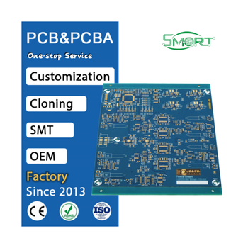
Industrial Automation Multilayer BGA Board
High-reliability multilayer FR4 PCB engineered for automation and robotic controls. Features precision BGA pads and tight impedance tolerance.
Reverse Engineering 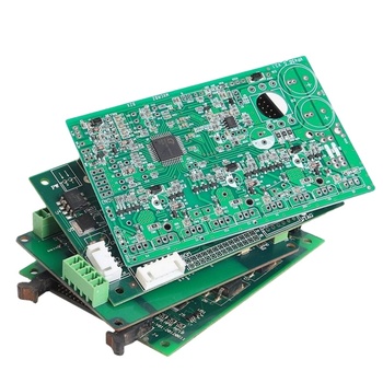
OEM/ODM PCB Cloning & Schematic Recovery
Full reverse engineering service for legacy electronics. Extract Gerber, schematic netlists, and bill of materials from physical golden samples.
Turnkey Mass Pro 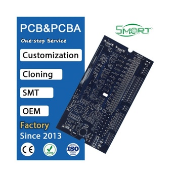
Turnkey Multilayer PCB Fabrication (2-12L)
Cost-effective bare board fabrication designed for volume consumer electronics, smart home appliances, and microcontrollers.
PLC & Control 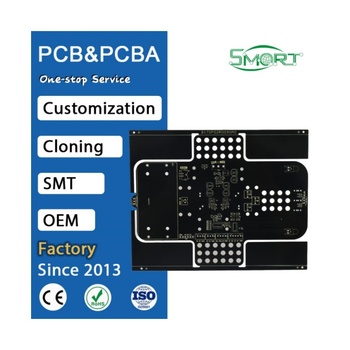
Industrial PLC Controller System Board
Ruggedized printed circuit board built to handle high electrostatic discharge (ESD) and industrial environmental stress.
Custom Stack-Up 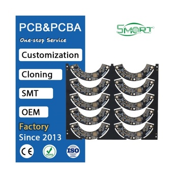
Multilayer PCB with Tailored Dielectric
Optimized 4-to-12 layer stack-up configurations tailored for low noise, differential pair impedance control, and RF shielding.
High-TG HDI 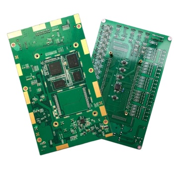
High-TG HDI Blind & Buried Via Board
Microvia technology and High-TG dielectric designed for compact smart devices, high-speed communication gear, and high computing cards.
Precision ENIG 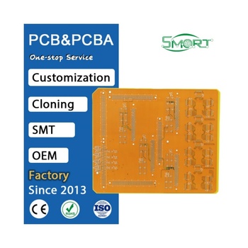
Precision FR4 Multilayer Board with ENIG
Ultra-flat surface co-planarity suitable for 0201 chip components, fine-pitch QFNs, and dual-row interconnect sockets.
Medical Grade 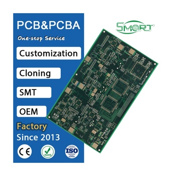
Cleanroom Medical Grade FR4 Board
Fabricated in climate-controlled environments with stringent ionic contamination testing. Suitable for diagnostic and monitoring apparatus.
Heavy Copper 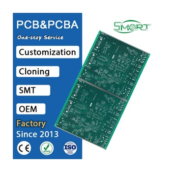
High-Power Heavy Copper Amplifier PCB
Supports 2 oz to 6 oz copper weight for power converters, audio subwoofers, motor drives, and industrial heating switches.
Rigid-Flex 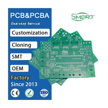
Automotive Grade Rigid-Flex Board
Combined polyimide flex circuit with rigid FR4 structural sections to eliminate wire harnesses and endure vibration.
Manufacturing Capabilities & Engineering Specifications
Shenzhen VUKO Electronics Co., Ltd. operates state-of-the-art production lines adhering to IPC-A-600 / IPC-6012 standards. Compare parameters below for your engineering qualification.
| Parameter | Standard Capability | Advanced / High-Precision |
| Layer Count | 1 – 8 Layers | 10 – 32 Layers (HDI Blind/Buried Vias) |
| Base Material | FR4 (Shengyi, KB, Nanya) | High-TG (TG170/180), Rogers, Polyimide, Aluminum |
| Board Thickness | 0.4mm – 2.4mm | 0.2mm – 4.0mm (±10% tolerance) |
| Copper Thickness | 0.5 oz – 2.0 oz | 3.0 oz – 6.0 oz (Heavy Copper) |
| Min. Trace Width / Spacing | 3.5 mil / 3.5 mil (0.09mm) | 3.0 mil / 3.0 mil (0.075mm) |
| Min. Finished Hole Size | 0.20 mm (8 mil) | 0.15 mm (Laser Microvia: 0.10 mm) |
| Surface Finishes | HASL, Lead-free HASL, OSP | ENIG (Immersion Gold), ENEPIG, Hard Gold Finger |
| Solder Mask Colors | Green, Blue, Red, Black, White, Yellow | Matte Black, Matte Green, Clear Mask |
| Quality Assurance Testing | Flying Probe E-test, Visual Check | AOI, Dedicated Fixture E-Test, X-Ray BGA, Impedance TDR |
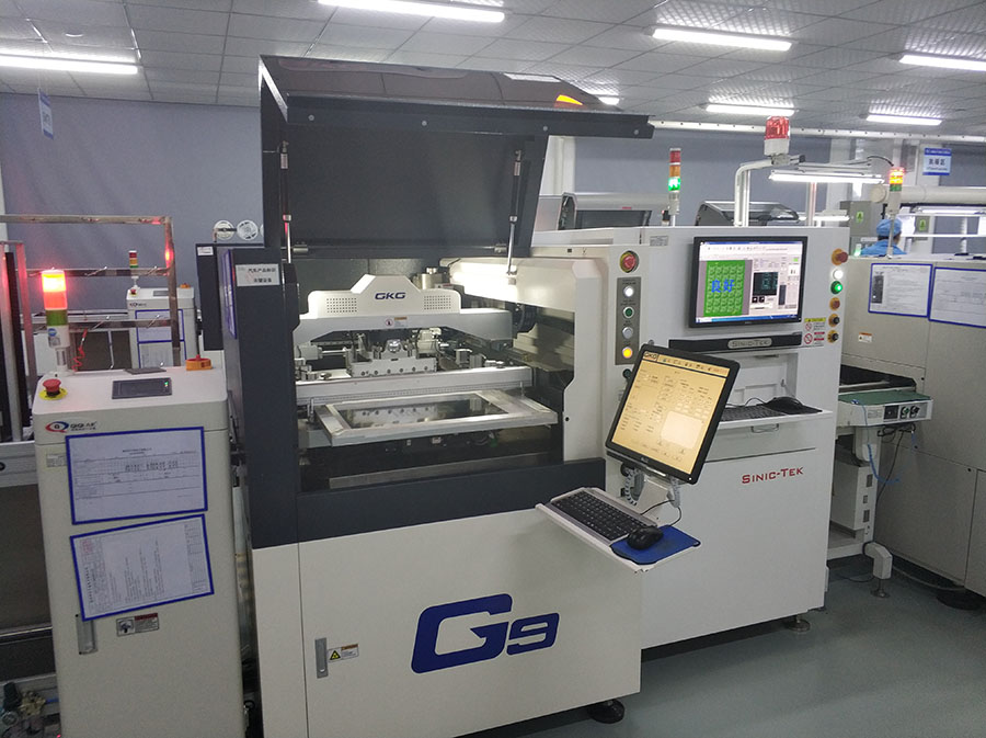
Factory Floor & Engineering Facilities
Shenzhen VUKO Electronics Co., Ltd. welcomes global OEM buyers for virtual audits and site visits. Traceable quality at every step.
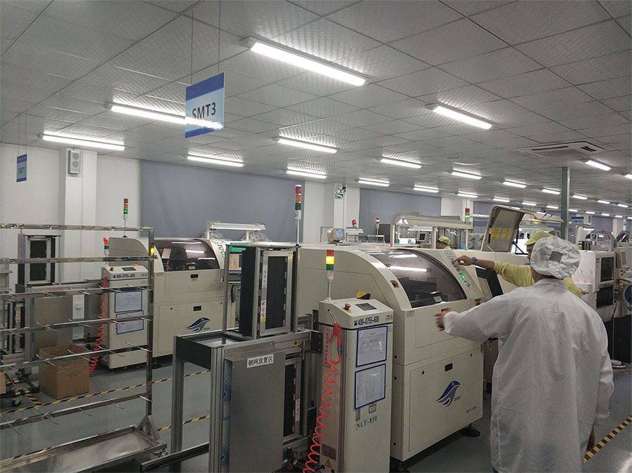
Engineering & Sales Headquarters
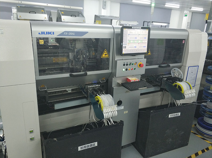
Technical Review & Operations Office
Sample Showcase & Testing Lab