Anatomy of a High-Efficiency Wireless Charging Transmitter PCBA
Understanding the critical circuit stages that dictate transfer efficiency, thermal margins, and electromagnetic performance.
A high-performance Wireless Charging Transmitter PCBA (Tx) is fundamentally an intelligent, digitally controlled resonant power inverter. Unlike generic power conversion boards, a wireless charging Tx PCBA must dynamically navigate volatile magnetic coupling coefficients ($k$), shifting load impedances, and tight electromagnetic limits. Every layer in the PCB stack-up—from copper distribution under the resonant LC bridge to shielding over sensitive baseband demodulators—directly dictates whether an end product achieves over 83% DC-to-DC transfer efficiency or suffers premature thermal shutdown.
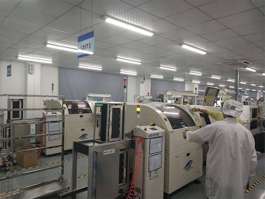
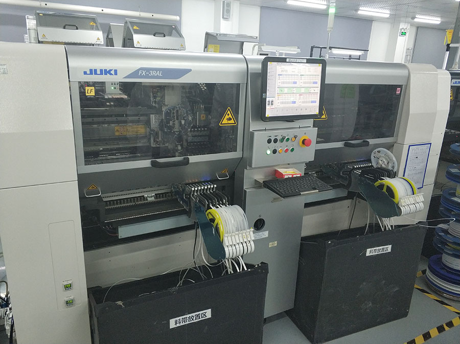
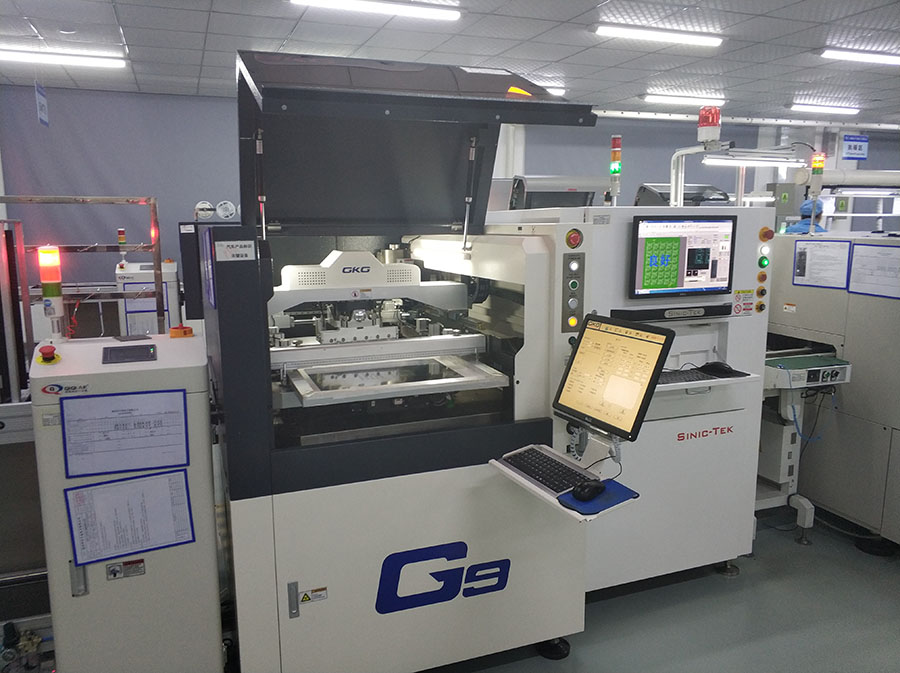
At Shenzhen VUKO Electronics Co., Ltd., we construct transmitter assemblies built around robust multi-stage architectures designed for maximum operational uptime across automotive cockpits, medical isolation enclosures, smart office furniture, and consumer electronics.
1. Digital Controller & Demodulation Core
Equipped with dedicated 32-bit DSP or ARM Cortex-M0 cores running hardware-accelerated FSK (Frequency Shift Keying) generation and differential ASK (Amplitude Shift Keying) demodulation. The MCU continuously monitors ping responses, negotiates Power Delivery contracts via Qi protocols, and modulates switching frequency or duty cycles dynamically.
2. High-Frequency Switching Inverter Bridge
Engineered in either Half-Bridge (cost-sensitive 5W–10W) or Full-Bridge (15W–50W high-dynamic range) topologies. Incorporating ultra-low $R_{DS(on)}$ (sub-10mΩ) N-channel MOSFETs or Gallium Nitride (GaN) power transistors minimizes switching dissipation and keeps junction temperatures well within safe operating areas during sustained peak loading.
3. Resonant LC Tank & C0G/NP0 Dielectrics
The heart of inductive resonant coupling. Uses multi-strand copper Litz wire coils (to eliminate skin and proximity effects at 100kHz–360kHz) coupled with specialized high-voltage C0G/NP0 ceramic capacitors possessing ultra-low Equivalent Series Resistance (ESR), preventing dielectric heat buildup under large circulating AC currents.
4. Dynamic Foreign Object Detection (FOD)
Prevents hazardous induction heating of stray coins, keys, or foil wrappers. Employs dual-stage protection: pre-power resonant curve characterization (measuring coil quality factor $Q$ and resonant frequency shifts) combined with milliwatt-accurate real-time power loss calculation during continuous transfer phases.
5. EMI Suppression & Filtering Network
Features multi-stage Pi filters, common-mode chokes, tuned RC snubber circuits across switching nodes, and strategic layout isolation between digital ground and noisy power loops. These deliberate design practices allow client products to clear CE, FCC Class B, and automotive CISPR 25 Class 5 certifications smoothly.
6. Multi-Protocol USB-C PD Front-End
Integrates USB Power Delivery (PD 3.0 / PPS) and Quick Charge (QC) physical layer decoders. The transmitter PCBA autonomously negotiates 9V, 12V, 15V, or 20V rail inputs from upstream adapters, converting bus voltages via high-efficiency synchronous buck-boost stages to precisely match dynamic target coil currents.