14+
Years Global Exporting
≤ 24h
DFM Review Turnaround
5 Pcs
Low Prototype MOQ
100%
E-Test & AOI Verification
Precision Manufacturing Portfolio
High-Reliability Capacitive & Embedded Hardware Solutions
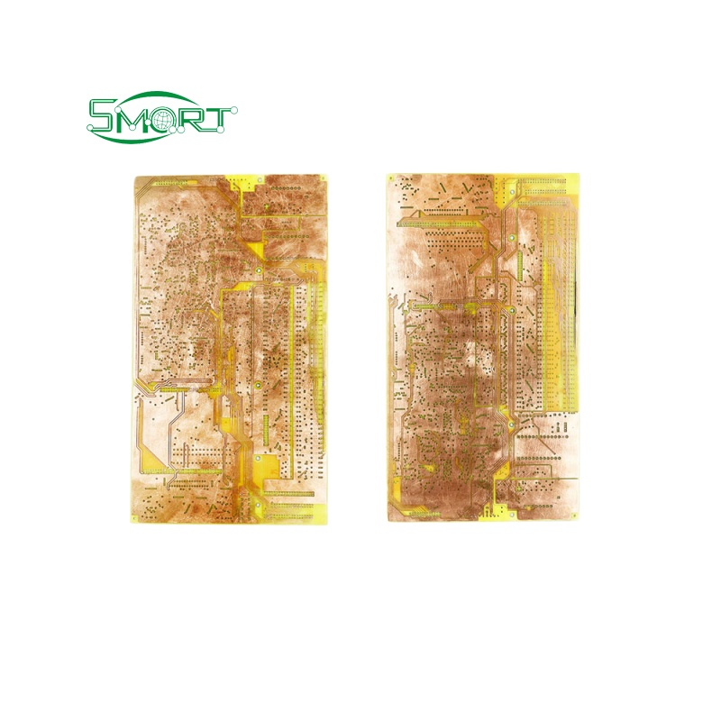
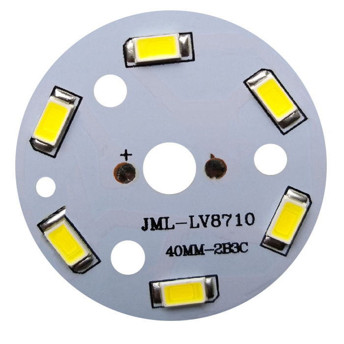
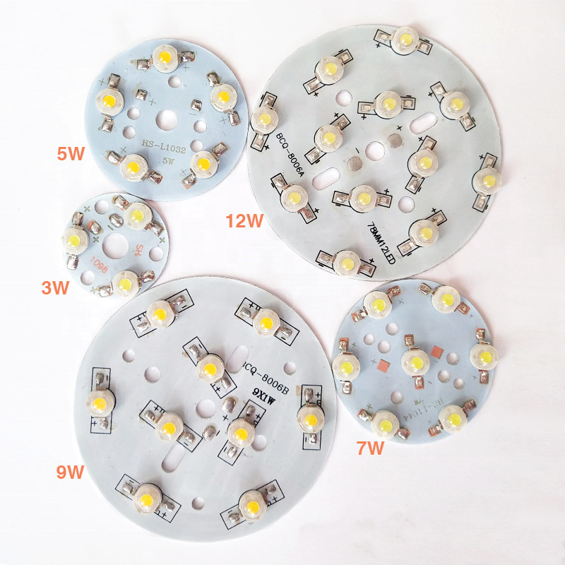
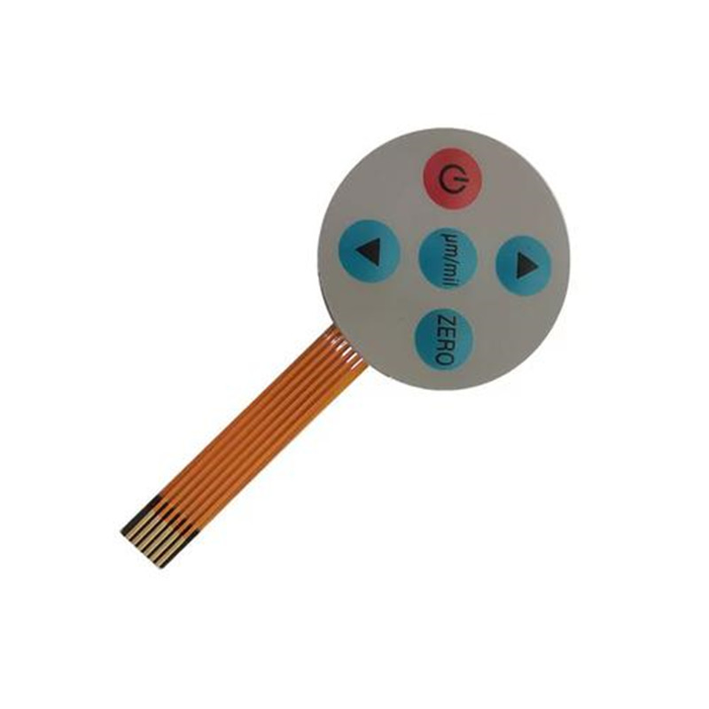
Explore our vertically integrated product ecosystem: from custom rigid and flexible sensor backplanes to fully assembled human-machine interface (HMI) modules.
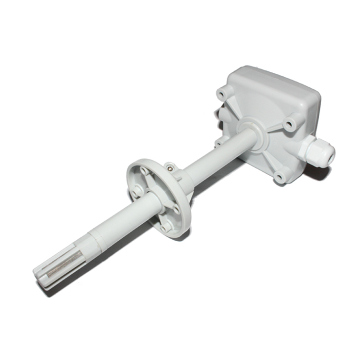
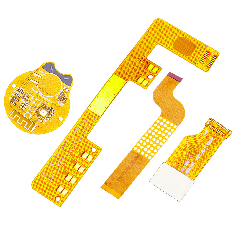
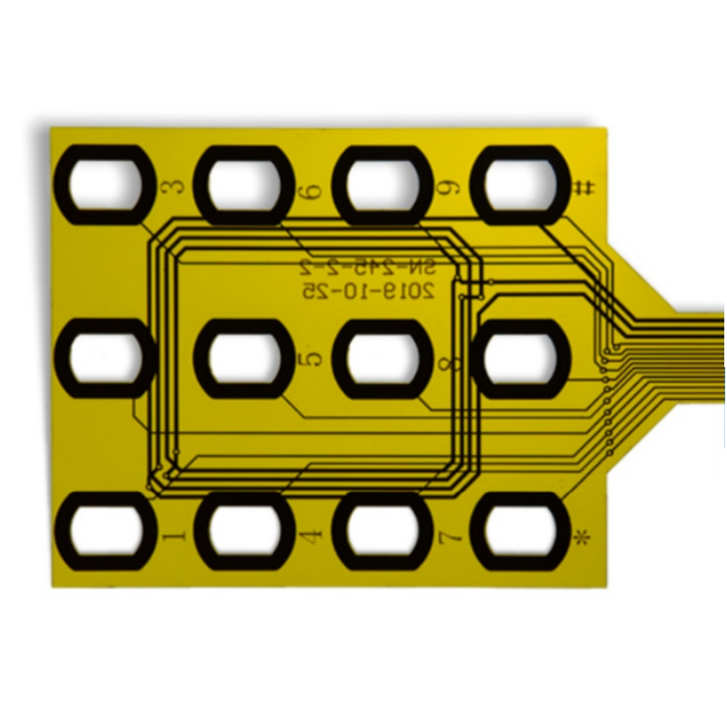
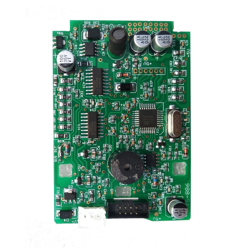
Engineering Architecture
Capacitive Sensing Mechanics: Design for Noise Immunity & Harsh Environments
A capacitive touch button relies on measuring the charge transfer across a printed electrode matrix. The introduction of a conductive target (such as a human finger) alters the mutual or self-capacitance ($C_s$) relative to the reference plane. Engineering a resilient capacitive touch interface demands comprehensive calibration of electrode geometry, overlay permittivity, and EMI shielding.
Parasitic Capacitance Mitigation
Traces routing from touch pads to controller ICs introduce parasitic capacitance ($C_p$). We deploy active guard rings and dynamic driven shields on inner PCB/FPC layers to maintain high Signal-to-Noise Ratio (SNR > 5:1), ensuring zero ghost triggers under high electromagnetic noise.
Dielectric Tuning Across Materials
Capacitance is inversely proportional to overlay thickness and directly proportional to the dielectric constant ($\varepsilon_r$). Whether integrating a 3.0mm toughened glass front panel ($\varepsilon_r \approx 7$), PMMA acrylic ($\varepsilon_r \approx 3.2$), or flexible PET overlays, our DFM team precisely calculates electrode pad diameters.
Water Rejection & Moisture Handling
Condensation or pooling water can create false capacitance differentials. We implement dual-electrode differential cross-sensing combined with auto-tuning MCU firmware baseline compensation to reliably differentiate between direct fingertip touches and pooled water droplets.
| Evaluation Parameter | Standard Membrane Switch | Capacitive Touch FPC Panel | Solid Rigid-Flex Touch PCBA |
|---|---|---|---|
| Mechanical Life Expectancy | 1,000,000 to 5,000,000 actuations | Solid-state (Virtually unlimited) | Solid-state (Virtually unlimited) |
| Sealing Rating Compatibility | IP65 (Perimeter Gasket Dependent) | IP67 / IP68 (Front Face Hermetic) | IP68 / IP69K (High-Pressure Washdown) |
| Overlay Material Variety | PET / Textured Polycarbonate | Tempered Glass, PMMA, Ceramic, Wood | Structural Polymers & Seamless Glass |
| Illumination Options | Embedded SMD LEDs / Light Guides | Capacitive Backlit Halo / RGB Capacitive | Dynamic Matrix Addressable Backlighting |
| Operating Temperature | -20°C to +70°C | -40°C to +85°C (PI Polyimide Core) | -40°C to +105°C (Automotive Grade) |
Industry Intelligence
Future Procurement Trends in Capacitive Touch & HMI Manufacturing
B2B procurement directors and senior hardware system designers are rethinking interface procurement. Here is how capacitive touch manufacturing is evolving over the next three to five years.
In-Mold Electronics (IME)
Shifting from planar membrane surfaces to deep 3D structural parts. IME directly combines functional capacitive traces and SMD LEDs into injection-molded plastics, slashing assembly steps and reducing structural weight by up to 70%.
Haptic Feedback Convergence
Capacitive touch eliminates mechanical travel, but users still demand tactile confirmation. Next-generation touch modules integrate ERM, LRA, or Piezo-ceramic actuators beneath the capacitive substrate to create localized, tactile click sensations upon touch detection.
Turnkey SMT & Controller Integration
Global OEMs no longer purchase bare sensor layers. The prevailing procurement model bundles capacitive sensing ICs (Cypress/Infineon, Microchip, Renesas), power distribution, and communication bus controllers (I2C/SPI/CAN) onto the same flexible circuit or PCBA.
Supply Chain Resilience & BOM Auditing
Procurement teams prioritize suppliers with internal component kitting teams. Sourcing partners that actively flag end-of-life (EOL) microcontrollers and validate pin-to-pin alternatives minimize line-stoppage risks caused by silicon shortages.
Enterprise Strengths
Why International OEMs Partner with Shenzhen VUKO Electronics
Located in the heart of Shenzhen’s advanced electronics manufacturing ecosystem, VUKO bridges complex engineering requirements with seamless export manufacturing.
24-Hour Engineering DFM & Rapid Prototyping
Our senior engineers review your Gerber files, BOM, and mechanical drawings within 24 hours. We evaluate layer stack-ups, pad spacing, via clearances, and impedance tolerance prior to cutting copper, catching errors early to prevent costly scrap and production delays.
End-to-End Vertical Manufacturing
No need to split orders across multiple vendors. VUKO delivers single-source manufacturing across Rigid PCBs (1–12+ layers), FPC flexible circuits, Aluminum core LED MCPCBs, SMT/DIP assembly, and custom membrane interfaces, ensuring consistent mechanical fits and trace integrity.
Turnkey BOM Component Sourcing & Traceability
We source authentic components directly from certified manufacturers and franchised distributors. Every IC, passive component, sensor, and connector is verified before placement, complete with anti-static packaging and full lot traceability for your peace of mind.
Rigorous In-House Testing Protocols
Every bare board passes 100% automated electrical testing (flying probe or bed-of-nails fixture). Assembled PCBAs undergo Automated Optical Inspection (AOI), X-ray testing for BGA packages, and custom functional circuit testing using dedicated test fixtures.
Low Prototype MOQ Scaling to Mass Output
We support your full product lifecycle with prototypes starting from just 5 pieces. You can validate fit, feel, and electrical performance at low volume before ramping into high-speed SMT assembly and volume panel fabrication.
Alibaba Verified & Trade Assurance Protected
As an onsite-verified supplier on Alibaba.com for over 14 years, our production processes, business credit, and trade track record are transparently validated, giving global buyers secure payment and reliable shipping protections.
Procurement Guidelines
Frequently Asked Questions on Custom Capacitive Touch Sourcing
Key technical and logistics questions addressed by our engineering and export trade specialists.
What design files and specifications are required to receive an accurate PCBA & capacitive touch quote?
For custom capacitive touch button modules and PCBAs, please provide:
1. Gerber Files: Standard RS-274X format along with NC drill files.
2. BOM (Bill of Materials): Complete with exact manufacturer part numbers (MPNs), component references, package footprints, and quantities.
3. Mechanical & Overlay Files: CAD drawings (DXF, STP) showing capacitive pad layouts, substrate thicknesses, graphic printing layers, and adhesive cutouts.
4. Testing Specifications: Programming hex files, functional test criteria, and jig requirements where applicable.
How do you tune capacitive touch buttons to operate through thick glass or acrylic overlays?
Sensitivity is directly influenced by the dielectric constant ($\varepsilon_r$) and thickness of the front overlay material. For overlays thicker than 3.0mm, our engineering team optimizes the surface area of the conductive copper/silver electrodes, minimizes parasitic trace capacitance, and recommends capacitive touch ICs with high internal charge-transfer resolution. In addition, we advise on the right optical clear adhesive (OCA) to prevent air gaps that degrade field strength.
Can VUKO produce curved or flexible capacitive touch sensor buttons?
Yes. By utilizing flexible printed circuit (FPC) technology with polyimide (PI) base materials, we build ultrathin (down to 0.057mm) capacitive sensor matrices. These flex arrays can easily conform to 3D contoured enclosures, automotive dash trim, cylindrical medical devices, and ergonomic consumer products.
What is your standard minimum order quantity (MOQ) and production lead time?
Our prototype MOQ starts at just 5 pieces for bare PCBs, FPCs, and complete PCBA runs. Quick-turn prototype bare boards can ship within 3–5 working days. Turnkey PCBA prototypes generally require 10–15 business days depending on component sourcing lead times, while high-volume production typically ships in 3 to 4 weeks.
How do you manage obsolete (EOL) components listed on client BOMs?
Our dedicated BOM sourcing team screens all components against global distribution databases during the initial 24-hour review. If an IC, passive component, or connector is flagged as obsolete or subject to extended factory lead times, our electrical engineers propose active, pin-compatible alternatives from top-tier brands for your approval before purchasing begins.
What certifications and quality control procedures protect finished goods?
All VUKO products comply with the European RoHS Directive and utilize UL 94V-0 fire-rated laminate materials. Our manufacturing processes strictly follow the ISO 9001:2015 quality management system. Assemblies undergo AOI inspection, in-circuit E-tests, thermal profiling, and comprehensive functional verification prior to vacuum anti-static export packing.
Accelerate Your Touch Interface Development
Submit your design specifications, Gerber packages, or BOM lists today. Our Shenzhen-based engineering team will deliver a comprehensive DFM assessment and formal quotation within 24 hours.