Enterprise Product Portfolio
Featured Membrane Interfaces & Integrated Electronics
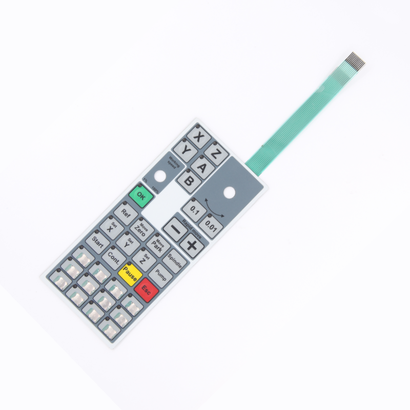
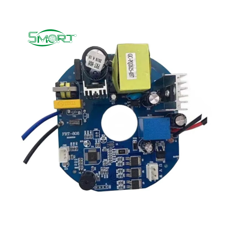
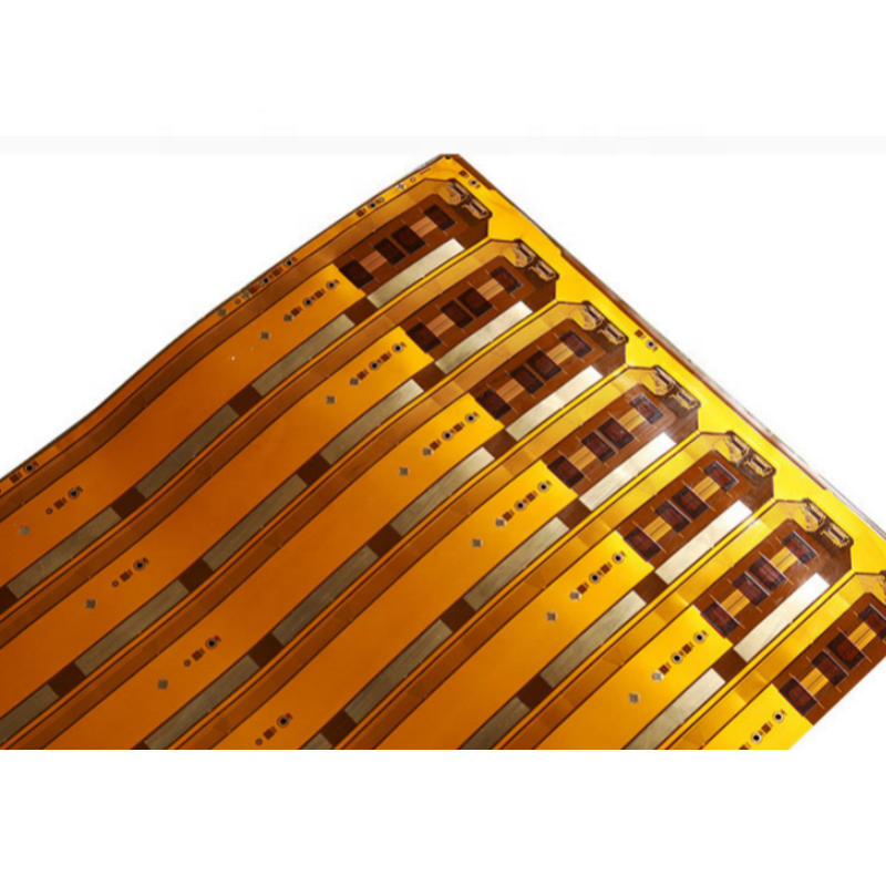
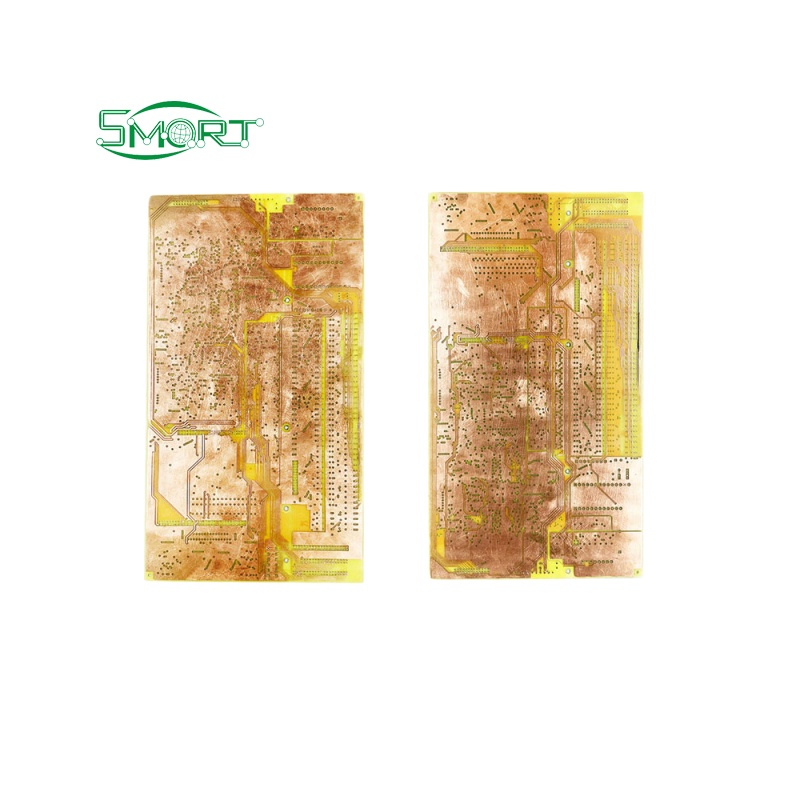
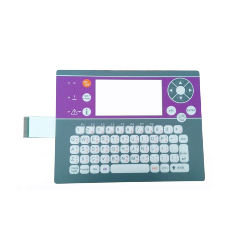
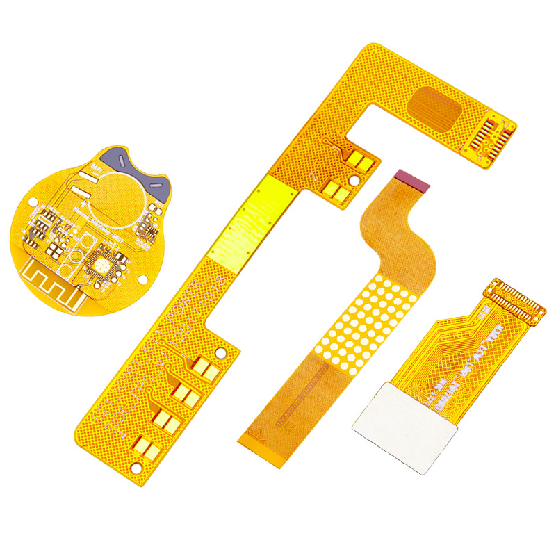
Precision-engineered flat non-tactile switch layers, custom flexible printed circuits, environmental sensor housings, and complete turnkey PCB assemblies manufactured to ISO 9001 and UL 94V-0 standards.
14+
Years Exporting Globally
>5,000,000
Actuations Per Switch
≤0.5 mm
Ultra-Low Layer Profile
24h
Engineering Review Window
Engineering Authority: Demystifying the Non-Tactile Membrane Switch Architecture
In modern electronic product design, the interface between operator and machine dictates both functional life expectancy and the user's perception of quality. While tactile membrane switches rely on stainless steel or polyester snap domes to provide physical click feedback, non-tactile membrane switches employ a completely planar, solid-state architecture. Actuation occurs with minimal travel—typically between 0.1mm and 0.4mm—as an upper conductive circuit pad is directly depressed into physical contact with a lower stationary circuit pad through an ultra-thin adhesive spacer opening.
Key Engineering Advantage: Eliminating metal domes removes mechanical metal fatigue from the equation. A precision-engineered non-tactile switch manufactured with premium silver or carbon inks on optical-grade biaxially-oriented PET can effortlessly exceed 5,000,000 actuation cycles without degradation of contact resistance or switch bounce characteristics.
Cross-Sectional Layer Breakdown
A high-reliability non-tactile interface consists of a carefully laminated composite sandwich designed to withstand moisture, aggressive solvents, and mechanical abrasion:
1. Graphic Overlay Layer: Autotype polyester (PET) or polycarbonate (PC), sub-surface printed to secure graphics, legends, and transparent LCD/LED windows against surface wear.
2. Top Circuit Substrate: Typically 0.125mm to 0.175mm heat-stabilized polyester film with screen-printed polymer thick film (PTF) silver conductor traces and carbon overcoat contact poles.
3. Dielectric Spacer Layer: High-cohesion acrylic adhesive carriers (such as 3M 467MP or 3M 468MP) die-cut with exact air-vent channels to prevent atmospheric pressure variations from inducing accidental contact closure.
4. Bottom Circuit Substrate: Matching PTF printed circuitry or, for demanding applications, a rigid FR4 PCB or polyimide flexible circuit (FPC) backer that provides structural stability.
5. Rear Mount Adhesive Layer: Industrial pressure-sensitive adhesive selected specifically for the surface energy of the end-product chassis (e.g., cast aluminum, ABS, or powder-coated steel).
Procurement Strategy 2026–2030
Future Sourcing Trends for Industrial HMI & Membrane Switches
How forward-thinking procurement directors, hardware architects, and supply chain managers are shifting their non-tactile membrane switch sourcing strategies to maximize return on investment and mitigate geopolitical risk.
One-Stop Turnkey Consolidation
Procuring raw membrane layers from one vendor, PCBs from a second, and SMT assembly from a third creates fragmented accountability. Leading OEM buyers are consolidating procurement with single-source Shenzhen manufacturers who fabricate bare PCBs, assemble driver boards, source passive BOM items, and print integrated membrane overlays under one roof.
Hermetic Sealing & Chemical Defense
Medical sterilization (alcohol, bleach, quaternary ammonia) and industrial washdowns demand continuous surfaces without crevices. Non-tactile switches offer unbroken flat facings that achieve IP67 or IP68 ratings easily. Procurement teams are moving away from mechanical pushbuttons toward seamless membrane overlays to simplify hygiene compliance.
Hybrid Touch & Haptic Convergence
While mechanical domes provide innate tactile response, modern non-tactile systems increasingly incorporate piezo haptic feedback drivers, back-mounted audio buzzers, or surface LEDs. This gives industrial operators tactile and acoustic confirmation without sacrificing the ultra-flat, zero-wear benefits of dome-less switch construction.
BOM Kitting & DFM Verification
Sourcing teams are actively demanding pre-manufacturing Design for Manufacturability (DFM) reviews. Identifying silver migration risks, optimizing tail pinouts, and recommending lead-free RoHS-compliant solder alternatives within the first 24 hours prevents costly production re-spins and accelerates time-to-market.
Technical Clarifications
Frequently Asked Questions on Non-Tactile Membrane Switch Sourcing
Direct engineering answers to assist hardware designers, component engineers, and procurement managers in making informed decisions.
What is the fundamental functional difference between tactile and non-tactile membrane switches?
The defining difference lies in the actuation mechanism and user feedback. Tactile switches incorporate formed metal or polyester snap domes that collapse suddenly when pressed, providing an unmistakable physical click. Non-tactile membrane switches lack this dome layer; they are completely flat, with circuit closure achieved by direct deflection of the top substrate against the bottom conductor across a 0.125mm spacer gap. Non-tactile designs offer a significantly longer operating life (>5 million cycles vs. ~1 million for tactile), completely flat washable profiles, and silent operation. They are usually paired with visual (LED) or acoustic (buzzer) feedback.
What design files and specifications must be submitted for an accurate engineering quote?
To receive a comprehensive DFM review and quotation within 24 hours, provide:
1. Graphic Overlay Artwork: Vector files (Adobe Illustrator .AI, CorelDRAW .CDR, or high-res vector PDF) specifying Pantone/RAL color codes, key embossing heights, and window clear/tint zones.
2. Circuit Schematic & Gerber: RS-274X Gerber files or mechanical DXF showing trace routing, contact pad coordinates, pinouts, and tail dimensions.
3. Mechanical Stack-up: Desired layer thicknesses, adhesive requirements (e.g., 3M 467MP vs. 3M 468MP), connector pitch (1.0mm, 2.54mm female housings, or bare ZIF ends), and operating environment parameters.
How do you prevent silver migration in high-humidity non-tactile switch applications?
Silver migration occurs when an applied DC potential in the presence of moisture leads to silver dendritic growth between adjacent conductor traces, causing short circuits. To prevent this, VUKO applies a 100% dielectric carbon overcoat over all silver conductors, maintains trace spacing exceeding 0.5mm wherever possible, and employs perimeter environmental adhesive gaskets. For extreme outdoor or washdown applications, we recommend replacing the printed silver PET circuit with an etched polyimide FPC or FR4 PCB base layer.
Can surface mount components (such as chip LEDs and resistors) be embedded into non-tactile switches?
Yes. Miniature surface-mount LEDs (0603, 0805, or 1206 footprints), current-limiting resistors, and light guides can be bonded directly to the circuit layer using isotropic conductive adhesives (silver epoxy) or soldered onto flexible polyimide (FPC) backings. The adhesive spacer layers are precision laser-cut to house the component height, keeping the finished top overlay completely flat and uniform.
What is the typical lead time from prototype approval to volume production?
Following DFM approval and artwork sign-off, functional membrane switch prototypes typically ship within 7 to 10 working days. For urgent fast-turn programs, quick-turn FPC and graphic samples can be produced in as little as 3 to 5 working days. Mass production lead times generally range between 12 and 18 working days, depending on BOM component availability, custom tooling requirements, and testing criteria.
How does VUKO ensure lot-to-lot color matching and dimensional stability?
We use calibrated X-Rite spectrophotometers to confirm Delta-E (ΔE) color variance remains strictly within commercial tolerance (ΔE < 1.0) under standardized D65 lighting. All PET and PC graphic overlay films undergo pre-shrink thermal stabilization baking prior to screen printing. This prevents heat-induced dimensional distortion during subsequent UV ink curing cycles, ensuring exact alignment with underlying circuit layers.