Alibaba.com Onsite-Verified Supplier Trade Assurance Order Protection [email protected]
🇺🇸 English🇩🇪 Deutsch 🇪🇸 Español🇫🇷 Français 🇵🇹 Português🇮🇹 Italiano 🇷🇺 Русский🇯🇵 日本語 🇰🇷 한국어🇸🇦 العربية 🇹🇷 Türkçe🇳🇱 Nederlands
High-Precision Laser Cutting • IPC-7525B • Fast Delivery to Poland

CE Certified SMT Stencil Factory & Supplier serving Wrocław

Precision laser-cut stainless steel foils, electropolished apertures, and specialized nano-coatings engineered for high-density automotive, industrial, and IoT Surface Mount Assembly across Lower Silesia.

Integrated SMT & Electronics Production Stack

Precision Stencils & Interconnected Electronics Catalog

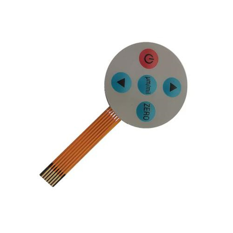
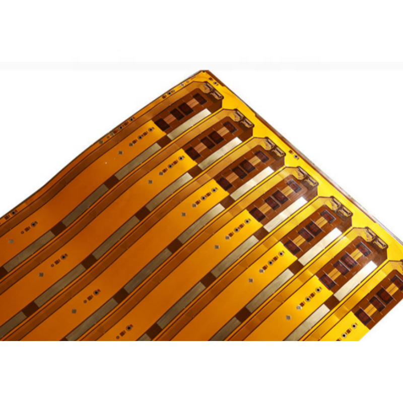
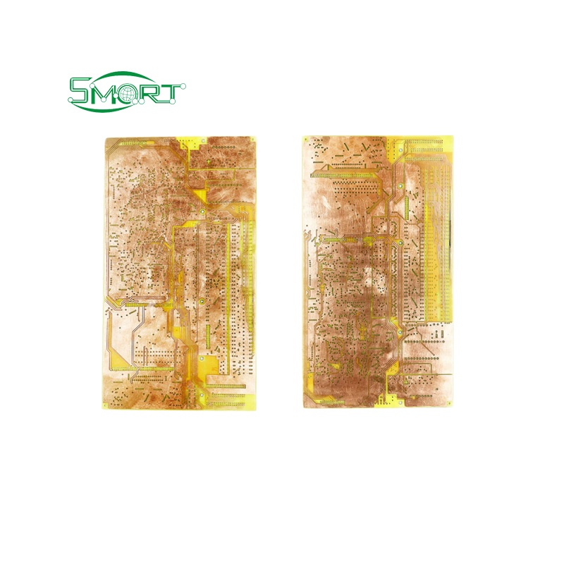
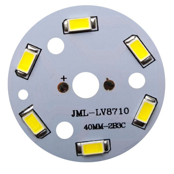
From micro-aperture laser stencils and high-TG multilayer bare boards to flexible circuits and human-machine interface assemblies, our Shenzhen manufacturing facility equips Wrocław EMS providers with end-to-end turnkey components under rigorous CE, RoHS, and ISO 9001 compliance standards.
±5 μm
Laser Aperture Cutting Tolerance
>0.66
Strict IPC-7525B Area Ratio Standard
24 Hours
Engineering DFM Review Turnaround
14+ Years
Global Export & Quality Traceability
Technical Whitepaper: Surface Mount Technology Tooling

State-of-the-Art Laser-Cut Stencil Fabrication Architecture

In modern Surface Mount Technology (SMT), over 65% of all soldering defects—including bridging, solder balling, tombstoning, and voiding—originate during the solder paste printing phase. For advanced contract electronics manufacturers (CEMs) and original equipment manufacturers (OEMs) operating within the Wrocław metropolis, maintaining optimal transfer efficiency demands world-class stencil engineering.

Material Metallurgy: High-Tensile German Stainless Steel (SUS304 / SUS316)
Standard chemical-etched or entry-grade laser stencils frequently suffer from internal residual stress, leading to localized foil warp and uneven snap-off during high-speed solder paste printing. Shenzhen VUKO Electronics utilizes exclusively fine-grain, cold-rolled surgical-grade austenitic stainless steel foils (SUS304 and SUS316H). This material possesses an ultra-dense grain structure (typically 2 to 5 μm crystal grain diameter compared to standard 10 to 15 μm industrial alloys), eliminating burr formation during fiber laser interaction.
Our fiber laser systems operate at a 1064 nm wavelength with dynamic pulse-width modulation (pulse duration < 20 picoseconds). This microscopic thermal interaction window prevents the creation of a wide Heat Affected Zone (HAZ). As a consequence, aperture sidewalls demonstrate an inherent taper angle of 1.0° to 1.8°, facilitating instantaneous paste release during vertical separation between the printed circuit board (PCB) surface and the stencil bottom foil.
Electrochemical Polishing & Plasma Fluoropolymer Nano-Coating
For micro-pitch surface mount assemblies featuring 01005 (0402 metric) chips, 0.35 mm pitch Wafer Level Chip Scale Packages (WLCSP), and ultra-fine quad-flat no-leads (QFN) footprints, untreated laser aperture sidewalls exhibit microscopic thermal scalloping. This microscopic roughness traps paste fluxes and fine tin-silver-copper (SAC305) powder spheres.
To eradicate aperture paste retention, our Wrocław-bound stencils can be configured with dual surface enhancements:
1. Electro-Chemical Polishing (EP): Controlled anodic dissolution removes micro-burrs and reduces surface roughness from Ra 0.8 μm down to less than Ra 0.2 μm, creating a mirror-like finish across all internal cut faces.
2. Hydrophobic & Oleophobic Nano-Coating: A monomolecular layer of organosilicon fluoropolymer is bonded directly to the stencil underside and aperture walls via chemical vapor deposition (CVD). This drops the surface tension to under 18 dynes/cm. Solder paste paste cannot wet the aperture edges, preventing under-stencil bridging and dramatically extending wiping intervals from once every 3 prints to once every 20-30 prints on automated DEK or MPM printing platforms.
IPC-7525B Mathematical Compliance & Aspect/Area Ratio Calculation
Every stencil aperture generated by our engineering department undergoes automated algorithmic Design-for-Manufacturing (DFM) verification based on the globally recognized IPC-7525B stencil design guidelines:
Design Parameter Mathematical Formula IPC-7525B Baseline Threshold VUKO High-Yield Tolerance Standard
Aspect Ratio (Width to Foil Thickness) Aspect Ratio = W / T > 1.50 ≥ 1.65 (Guaranteed release for 0201 passives)
Area Ratio (Aperture Opening to Wall Area) Area Ratio = (L × W) / [2 × (L + W) × T] > 0.66 ≥ 0.68 for standard; ≥ 0.55 with Nano-Coating
Round Apertures (BGA / Micro-Vias) Area Ratio = D / (4 × T) > 0.66 ≥ 0.65 (Enables down to 0.22 mm round pads)
Laser Beam Kerf Diameter Spot Size Diameter (ø) 25 μm – 35 μm 18 μm ± 2 μm (High-brightness Fiber Diode)
Aperture Positional Precision ΔX, ΔY over 600 mm × 600 mm ± 12.5 μm ± 5.0 μm Laser Interferometer Verified
Where W = aperture width, L = aperture length, T = stencil foil thickness, and D = circular aperture diameter. By mathematically pre-screening customer Gerber RS-274X and ODB++ files, our CAM software automatically compensates for thermal expansion coefficients and advises when to implement step-down pockets or home-plate geometries to eliminate solder ball splashing.
Dolnośląskie Regional Integration

Precision SMT Tooling for the Wrocław Electronics Hub

Wrocław has firmly established itself as Poland's premier high-tech powerhouse and the beating heart of Lower Silesia (Dolny Śląsk). From the sprawling electromobility developments around Kobierzyce and Bielany Wrocławskie to the advanced R&D centers in Wrocław Technology Park (Wrocławski Park Technologiczny - WPT), high-reliability electronics assembly demands precision tooling matched to local production rigors.

Electromobility & Green Tech

EV Battery Management (BMS) & Inverters

The concentration of European gigafactories and automotive component makers along the A4 corridor near Kobierzyce requires zero-ppm defect rates. Our stepped stencils facilitate printing thick solder deposits on high-amperage copper shunts and power MOSFETs while concurrently depositing ultra-thin paste volumes on adjacent microcontroller pins within BMS mainboards.

Industrial Automation & Drives

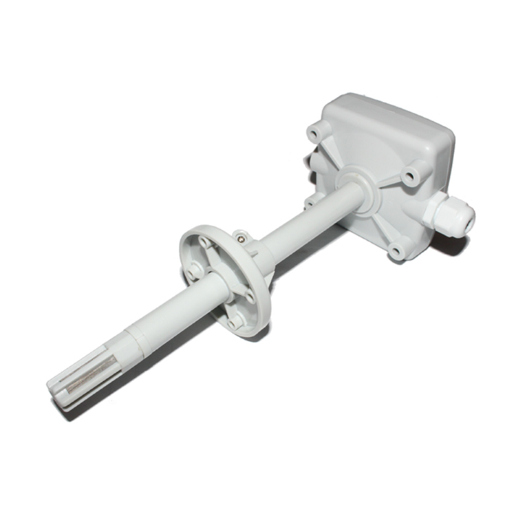
PLC Controllers, Inverters & Sensor Heads

Wrocław's robust automation engineering ecosystem builds ruggedized programmable logic controllers and frequency inverters. We deliver heavy-foil stencils (up to 250 μm) and aluminum core MCPCBs engineered to handle high current, cyclic vibration, and wide operational temperature spans in European industrial robotics installations.

Smart Metering & Telecom

IoT Nodes & 5G Gateway Infrastructure

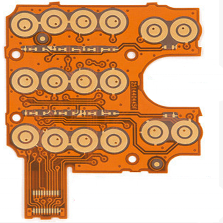
IoT device design teams based in Krzyki, Fabryczna, and surrounding tech hubs demand rapid micro-pitch prototypes. Our electropolished stencils ensure crisp print release on dense 0.4 mm pitch RF transceivers, matching seamlessly with our flexible circuit (FPC) tails and custom tactile membrane interface switches.

Industry 4.0 & Manufacturing Forecast

Technology Trajectories for Wrocław EMS Lines (2025–2030)

The continuous convergence of miniaturization, sustainable manufacturing directives, and automated quality assurance is shifting how production engineers across Poland approach the solder paste printing process.

Sub-0201 & Micro-BGA Expansion

With automotive infotainment and edge-AI compute modules adopting sub-0.3 mm pitch packaging, mechanical chemistry must give way to advanced laser ablation. Next-generation stencils combine 70 μm ultrathin foils with hydrophobic plasma films to ensure uniform paste release without aperture plugging or solder bridges.

RoHS, REACH & Low-Temp Soldering

EU environmental mandates are pushing lower soldering temperatures (Bismuth-Tin alloys) and lead-free fluxes across Lower Silesia. These paste formulations present distinct rheological profiles and wetting characteristics, requiring custom chamfered aperture profiles to maintain optimal print definition.

Closed-Loop SPI Integration

Industry 4.0-compliant SMT lines in Poland utilize automated 3D Solder Paste Inspection (SPI) directly feeding paste volume data back into screen printers. High-precision laser stencils manufactured with sub-5 micron repeatable tolerances provide the structural consistency required to prevent false SPI alarms.

Enterprise Strengths & Capabilities

Why Engineering Teams Work Directly with VUKO Electronics

Combining over 14 years of direct export excellence on Alibaba.com with world-class production facilities in Shenzhen, we provide Wrocław manufacturing buyers with verified quality, rapid turnaround, and end-to-end hardware solutions.

Verified Direct Manufacturer

Onsite-audited production facilities with direct factory pricing, eliminating middleman distributor markups.

Rigorous Multi-Stage QC

Optical measurement, laser interferometer verification, AOI testing, and strict electrical verification across every run.

Rapid DFM Review (24h)

Experienced CAM engineers evaluate aperture area ratios, fiducial markings, and aspect limits before fabrication.

Trade Assurance Protection

Payment security, full compliance documentation, and guaranteed on-time delivery backed by verified credentials.

Procurement & Engineering FAQ

Frequently Asked Questions for Wrocław Purchasing Managers

Clear answers regarding international shipping, European Union compliance, design modifications, and framing specifications for your factory lines.

How do you manage express delivery and customs clearance into Wrocław?
We partner with premier international logistics couriers including DHL Express, FedEx Priority, and UPS to deliver directly to facilities throughout Wrocław, Kobierzyce, Bielany Wrocławskie, and the entire Dolnośląskie voivodeship. Typical transit time from our facility via air cargo directly to Wrocław Copernicus Airport (Port Lotniczy Wrocław - WRO) or European central hubs is 3 to 5 business days. All shipments can be managed under DAP or DDP (Delivered Duty Paid) Incoterms, complete with commercial invoices, HS codes, and CE declarations for immediate clearance.
What stencil frame sizes and quick-release tension systems do you support?
We support both permanently mounted cast-aluminum frames and frameless foils for universal pneumatic tensioning systems. Standard frame dimensions include 370 × 470 mm, 420 × 520 mm, 550 × 650 mm, 584 × 584 mm (23" × 23"), 736 × 736 mm (29" × 29"), and custom European printer profiles. For frameless systems, we supply pre-punched foils compatible with VectorGuard®, ZelFlex, and Alpha Tetra standard self-tensioning frames utilized by high-volume Polish EMS facilities.
What files are required to manufacture an exact SMT stencil?
To ensure zero ambiguity, please supply your top and bottom Solder Paste layers (typically .GTP and .GBP extensions in standard Gerber RS-274X format) or ODB++ manufacturing databases. We also require the board outline layer (.GKO or .GM1), silkscreen references, and drill files if fiducials or mechanical mounting pins are to be registered. If you need step-up or step-down stencils, please clearly provide an engineering drawing detailing pocket depths and specific component reference designators.
Are your SMT stencils CE certified and compliant with EU RoHS / REACH standards?
Yes. All stencils and related electronic components manufactured by Shenzhen VUKO Electronics Co., Ltd. are certified in compliance with the European Union's CE directives, RoHS (Directive 2011/65/EU and amendment 2015/863), and REACH regulations (EC 1907/2006). Certificates of Conformance (CoC), material traceability sheets, and third-party laboratory test reports are provided upon request with every production lot.
How are fiducials treated for automatic vision alignment on Panasonic, Yamaha, and ASM printers?
Fiducials can be cut as full cut-through holes or half-etched cavities. To maximize optical contrast under automated vision cameras, we recommend half-etched fiducials on the board-contact side filled with durable, solvent-resistant black epoxy resin. This produces a non-reflective, high-contrast target against the brushed metallic stainless steel surface, preventing optical alignment errors on high-speed SMT line setups.
Can VUKO handle our complete turnkey electronics requirements beyond stencils?
Absolutely. Stencils represent just one facet of our one-stop electronic hardware capabilities. We specialize in rigid multilayer PCB fabrication (up to 12+ layers), flexible printed circuits (FPC), metal-core aluminum PCBs, turnkey PCBA (surface mount + through-hole assembly), custom membrane switch keypads, and complete BOM component procurement. Wrocław customers frequently combine bare boards, stencils, and assembled sub-modules on a single purchase order to streamline European import logistics.

Accelerate Your Wrocław SMT Production Yields Today

Submit your Gerber files or BOM documentation today for an in-depth engineering review, DFM verification, and a competitive direct factory quote delivered within 24 hours.