Precision Manufacturing Portfolio
High-Spec Prototyping Modules & Hardware Solutions
Engineered for high-reliability applications, quick-turn verification, and seamless scaling from single proof-of-concepts to series production batches.
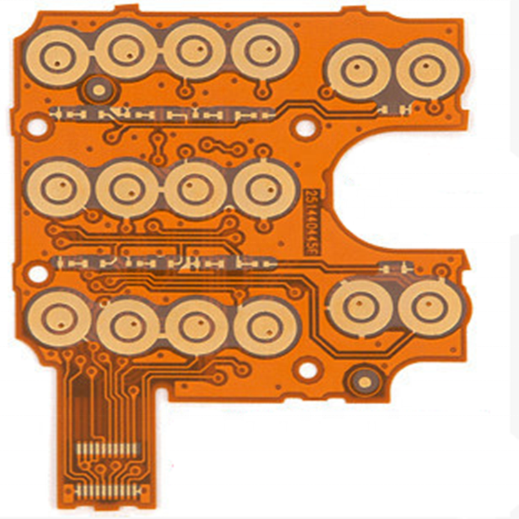
Shenzhen Factory Custom FPC FPCB Flexible PCB Board, Flexible Printed Circuit, FFC Tail, High Flexibility for Membrane Switch
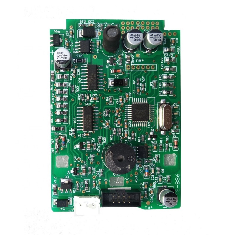
Shenzhen PCBA Manufacturer Custom Printed Circuit Board Assembly SMT PCB PCBA Prototype & Mass Production Service
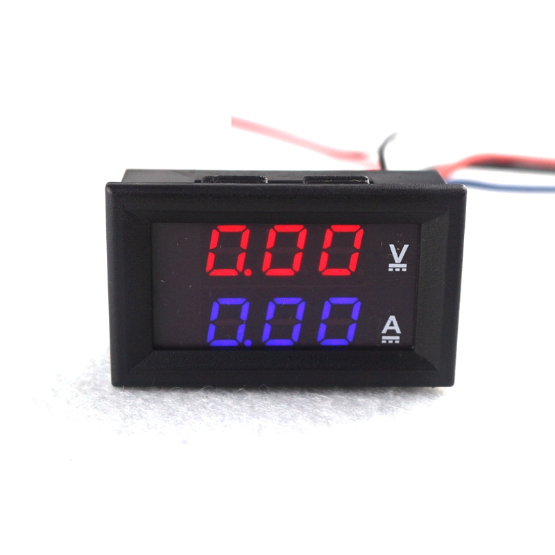
DC 100V 1-10A Digital Voltmeter Ammeter Dual Color LED Panel Meter Red Blue Voltage Current Tester
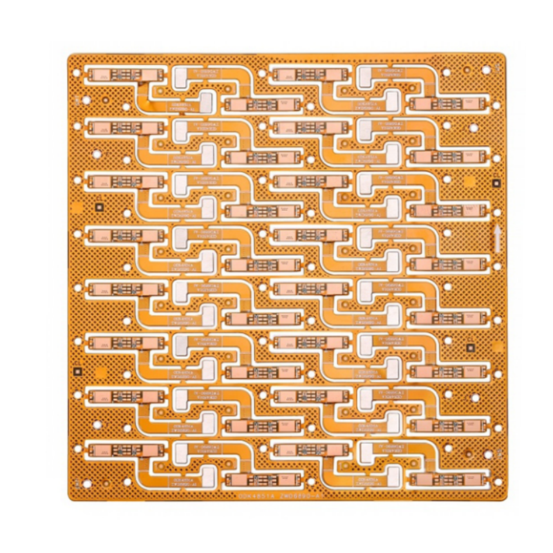
Custom FPC PCBA Service, Flexible Printed Circuit Board SMT Assembly, One Stop OEM Flex PCB Manufacturing
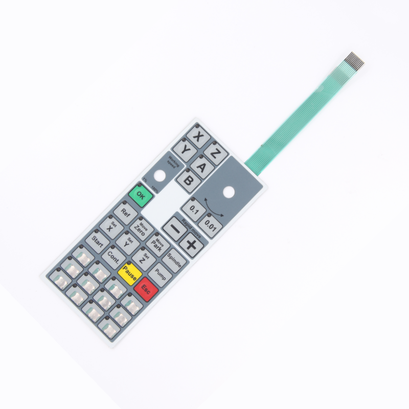
Shenzhen Factory Custom Membrane Switch, PET PC PVC Flexible Keypad, Silver Ink Circuit, FPC FFC Tail, Custom Logo Panel
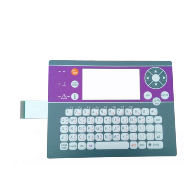
Custom Membrane Switch Keypad, Embossed Tactile Metal Dome, IP67 Waterproof 3M Adhesive Graphic Overlay for Industrial Control
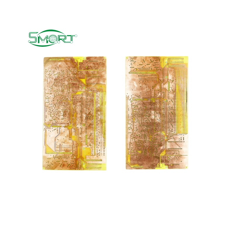
Smart Electronics Custom Multilayer PCB Board OEM Service FR4 Base Material 1oz Copper Thickness Custom PCB Fabrication
Engineering Whitepaper
High-Mix Prototyping and SMT Assembly for the Brainport Ecosystem
Bridging design-in labs at High Tech Campus Eindhoven (HTCE) and Brainport Industries Campus (BIC) with zero-defect fabrication standards.
Eindhoven stands as the undisputed heart of European deep-tech hardware. Anchored by world leaders such as ASML, Philips Healthcare, NXP Semiconductors, and an expansive tier-1 supplier network across the Brainport region, the demands placed upon bare circuit boards and surface-mount assemblies surpass typical commercial parameters. Rapid innovation cycles demand immediate Design for Manufacturability (DFM) verification, stringent signal integrity handling, tight physical tolerances, and reliable multi-layer thermal dissipation.
24 Hours
Pre-Production DFM & DRC Report
≥ 99.8%
First-Pass SMT Yield Rate
5 Pcs
Agile Pilot Run MOQ
100%
AOI, Flying Probe & E-Testing
Hardware development in Brainport is characterized by tight R&D sprint cadences. Whether engineering an optical sensing sub-assembly, a high-speed FPGA processing backplane for semiconductor wafer handling, or a bio-compatible wearable diagnostic patch, engineers cannot afford repeated fabrication revisions caused by undiscovered footprint mismatches or uncalculated thermal expansion coefficients. Our agile manufacturing model bridges direct Shenzhen production velocity with the exact mechanical, electrical, and regulatory requirements expected by Eindhoven purchasing directors and lead system architects.
| Engineering Parameter | Standard Commercial PCB | High-Tech Eindhoven Specification (Our Benchmark) | Inspection & Verification Method |
|---|---|---|---|
| Layer Count & Stackup | 1 – 4 Layers (FR4 standard) | 2 – 32 Layers (High-Tg FR4, Rogers, Polyimide, Hybrids) | Cross-section microsectioning & X-ray layer verification |
| Line Width / Spacing | 5 / 5 mil (0.127mm) | Down to 2.5 / 2.5 mil (0.0635mm) for fine-pitch HDI BGA | Laser direct imaging (LDI) & Automated Optical Inspection (AOI) |
| Impedance Control | ± 10% tolerance | ± 5% tight tolerance (Single-ended 50Ω, Diff 90/100Ω) | TDR (Time Domain Reflectometry) test coupons per panel |
| Via Architecture | Through-hole mechanical drilling | Microvia (Laser-drilled), Blind/Buried, Via-in-Pad Plated Over (VIPPO) | 3D X-ray inspection (AXI) & electrical testing |
| Surface Finishes | HASL / Leaded HASL | Electroless Nickel Immersion Gold (ENIG), ENEPIG, Immersion Silver, OSP | XRF plating thickness analyzer (IPC-4552 standard) |
| SMT Placement Capability | 0603 passive packages, 0.8mm BGA | 01005 passives, 0.3mm pitch micro-BGA, QFN, ultra-fine CSP | Solder Paste Inspection (SPI) + Multi-angle 3D AOI |
Regional Integration
Localized Application Scenarios in North Brabant
Tailored manufacturing implementations aligned directly with regional cluster competencies across Eindhoven, Veldhoven, Best, and Helmond.
Semiconductor Lithography & Vacuum Metrology
Veldhoven and Eindhoven host the world's most sophisticated lithography and wafer-handling equipment clusters. Auxiliary telemetry boards, ultra-clean digital ammeter/voltmeter diagnostic fixtures, and low-outgassing multilayer FR4 substrates are required for vacuum chambers and cleanroom testing. Our vacuum-sealed, ionic-tested boards conform to rigorous cleanliness benchmarks that minimize contamination hazards in sub-nanometer optoelectronic environments.
Mechatronics, AGVs & High-Torque Robotics
The Brainport Industries Campus relies heavily on multi-axis automated guided vehicles (AGVs), advanced pick-and-place end-effectors, and robotic drive units. These systems utilize heavy-copper (2oz to 6oz) multi-layer boards to dissipate immense current loads without thermal breakdown. By pairing heavy-copper traces with custom FPC cables, robotic arms maintain dynamic bend cycles exceeding 500,000 actuations without signal distortion or conductor micro-fracturing.
MedTech Diagnostic Consoles & Patient Interfaces
Along the medical innovation corridor running through Best and Eindhoven, patient monitoring consoles and diagnostic imagers require robust human-machine interfaces (HMI). Our custom embossed tactile membrane switches and sealed IP67-rated graphic keypads resist repeated chemical disinfection (isopropyl alcohol, hospital detergents) while maintaining tactile feedback. Interfaced with flex-circuit tails, these assemblies eliminate bulk wiring inside compact clinical enclosures.
AgriTech & Precision Greenhouse Automation
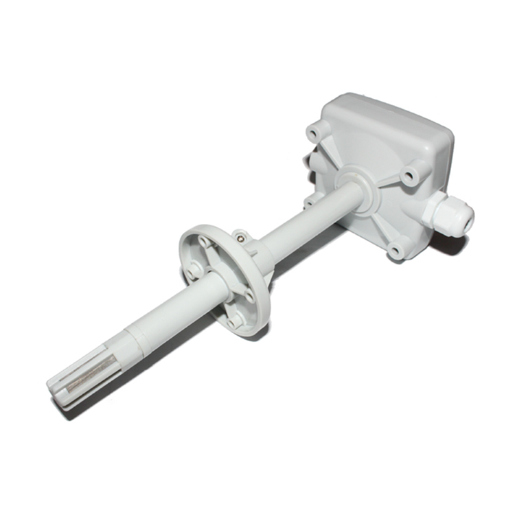
Surrounding the high-tech Brainport periphery, industrial greenhouse complexes and agro-robotic developers implement distributed environmental monitoring networks. Smart duct-type humidity sensor enclosures, coupled with conformal-coated IoT circuit assemblies, withstand extreme humidity fluctuations, fertilizer vapor exposure, and wide diurnal temperature swings without calibration drift.
Power Electronics & High-Flux LED Illumination
Modern EV charging infrastructure in Helmond’s Automotive Campus and industrial UV curing modules demand high-efficiency heat dissipation. Aluminum-backed metal-core PCBs (MCPCB) offering 1.0 to 5.0 W/m·K dielectric conductivity direct heat away from gallium-nitride (GaN) power switches and high-output LED arrays, securing extended operational lifespans and preventing junction thermal degradation.
Rapid University & R&D Spinoff Prototyping
Spinoffs from TU Eindhoven (TU/e) and TNO often enter rapid proof-of-concept stages where functional hardware must be built within days. Our prototype service accepts single-digit orders with no tooling penalties, offering turnkey component kitting, stenciling, pick-and-place assembly, and automated testing to accelerate grant milestone demonstrations and venture financing validations.
Future Roadmaps
Trends Shaping PCB & PCBA Engineering in Eindhoven
How evolving mechanical and RF standards dictate smarter material selections and layout architectures.
1. Sub-50μm HDI Geometries
As microcontrollers, AI accelerators, and high-performance FPGAs transition to 0.4mm pitch ball grids, conventional drilling fails. Blind and buried laser microvias (stacked or staggered) allow complex fanouts within tight 8-to-16-layer budgets without layer count bloating.
2. Rigid-Flex Space Reduction
Eindhoven engineers increasingly eliminate discrete wiring harnesses. By utilizing 4-layer rigid sections integrated with 2-layer dynamic flex circuits, mechatronic modules drop 35% in overall mass while removing high-vibration failure points caused by loose pin headers.
3. Thermal Clad Hybrids
High-voltage battery management systems (BMS) for robotics pair logic controllers with heavy power stages. Hybrid stackups, where high-conductivity ceramic-filled prepregs bond to aluminum or copper substrates, allow microcontrollers and switching MOSFETs to share one compact PCB.
4. Turnkey DFM BOM Cleansing
Global semiconductor availability fluctuations require proactive engineering. Our pre-production DFM verifies alternate footprints for passive components and microcontrollers before etching copper, preventing unexpected line stoppages during assembly.
Factory Capabilities
Why Eindhoven Engineering Teams Bridge with Us
Combining the world-class electronics supply base of Shenzhen with direct, engineer-to-engineer European communication standards.
14+ Years of International Direct Export
We have spent over a decade delivering bare PCBs, turnkey SMT assemblies, FPC flex interconnects, and membrane switches to hardware companies across the EU, UK, and North America. Every shipment includes full traceability documentation, material certificates (UL 94V-0, RoHS, REACH), and cross-section micrographs upon request.
24-Hour Comprehensive DFM & BOM Review
Your Gerber files, centroid pick-and-place data, and bill of materials undergo scrutiny by experienced CAM engineers within 24 hours of submission. We identify trace/space bottlenecks, acute acid traps, pad size mismatches, and unseated micro-vias before panels ever reach chemistry tanks, eliminating expensive re-spins.
Complete Turnkey Sourcing & Anti-Counterfeit Audits
Save weeks of procurement overhead. Our supply chain specialists source passive components, microcontrollers, optoelectronics, sensors, and mechanical hardware directly through franchised distributors and vetted factory lines. Incoming components undergo microscopic authenticity inspection and pin verification prior to feeder loading.
Full In-House Quality Verification
Every board produced must clear rigid validation gates. Bare boards are subject to automated flying probe or dedicated electrical fixture continuity/isolation tests. PCBA runs undergo 3D solder paste inspection (SPI), multi-angle automated optical inspection (AOI), and functional testing to custom test fixtures and programming firmware.
HMI & Complete Sub-System Integration
Beyond bare circuit fabrication, we uniquely specialize in complete front-end interfaces. We manufacture graphic overlay panels, metal dome membrane switch arrays, embedded LED capacitive touch units, and custom flexible printed circuits under one roof. Engineers receive cohesive, tested human-machine sub-assemblies ready for chassis installation.
Low-MOQ Agility to Volume Scalability
We remove commercial gatekeeping for high-tech ventures. Begin with an engineering sample order of 5 pieces for early bench validation, move seamlessly into 100-to-1,000 piece pilot batches for field validation, and scale smoothly to mass automated production runs without switching fabrication partners or requalifying tooling sets.
Procurement Guide
Frequently Asked Questions by Eindhoven Hardware Teams
Clear, direct answers regarding logistical timelines, DFM requirements, compliance, and trade guarantees.
Q1 What documentation is required for an immediate and accurate DFM quote?
For bare PCB fabrication quotes, please supply complete Gerber files in RS-274X format or ODB++ archives, accompanied by an Excellon NC drill file and a fabrication drawing specifying layer stackup, copper weight (outer and inner), dielectric thickness, surface finish (e.g., ENIG 2u" Au / 120u" Ni), solder mask color, and panel routing tolerances. For complete PCBA turnkey quotes, include an itemized Bill of Materials (BOM) in Excel format with complete manufacturer part numbers (MPNs), reference designators, package footprints, and centroid/pick-and-place XY coordinate data.
Q2 What are the typical turnaround and transit timelines to the Brainport Eindhoven region?
Standard quick-turn bare PCB prototypes (2 to 6 layers) can be fabricated in 3 to 5 business days, with expedited 48-hour service available for critical sprints. Complex multi-layer HDI (8 to 16 layers) typically requires 6 to 9 days. Turnkey PCBA prototypes generally require 10 to 14 days, including component sourcing and custom laser stencil preparation. We ship via express priority air logistics (DHL, FedEx, UPS) directly into Eindhoven Airport (EIN) or Amsterdam Schiphol (AMS), delivering directly to your door at High Tech Campus, Brainport Industries Campus, or nearby sites within 3 to 4 business days from dispatch.
Q3 How do you guarantee compliance with European Union environmental standards (RoHS / REACH)?
All laminates, solders, flux chemistries, surface plating baths, and overlay adhesives used in our manufacturing process strictly comply with EU Directive 2011/65/EU (RoHS 2.0 / RoHS 3) and Regulation (EC) No 1907/2006 (REACH). We do not employ restricted hazardous substances, such as lead, mercury, cadmium, hexavalent chromium, PBBs, PBDEs, or listed phthalates. Official Declarations of Conformity (DoC) and certified SGS third-party laboratory test reports are provided with every initial production shipment for your QA records.
Q4 How does your team handle component obsolescence or long-lead IC shortages?
During our initial 24-hour BOM scrub, our component engineering team checks active lifecycle status across all BOM line items. If any passive component, microcontroller, or specialty sensor is identified as End-of-Life (EOL), Not Recommended for New Designs (NRND), or subject to unacceptable factory lead times, we recommend functionally equivalent, pin-compatible alternatives from tier-one manufacturers (e.g., TI, STMicroelectronics, NXP, Microchip). No component substitution is ever approved or ordered without explicit written consent from your hardware design team.
Q5 What financial and payment protections are available for Dutch corporate buyers?
To provide complete fiscal security for our international clients, projects can be processed securely through Alibaba.com Trade Assurance. This escrow service guarantees payment security, delivery on the agreed schedule, and contractual quality compliance. In addition, established corporate clients and research organizations can access standard commercial wire transfer (T/T), PayPal, and tailored milestone payment structures following initial credit review.
Initiate Your Next High-Tech Prototype Build
Collaborate with an engineering manufacturing partner that understands the precision, speed, and reliability demands of Eindhoven's hardware ecosystem. Send your Gerber and BOM data now for an engineer-led DFM audit and custom quotation within 24 hours.