Featured Manufacturing Products & Modular Assemblies
Complementary electronic manufacturing materials, custom FPC solutions, and industrial components engineered under rigorous quality benchmarks.
SMT Stencil Dynamics in High-Yield Surface Mount Assembly
An in-depth metallurgical and process engineering evaluation of solder paste deposition for advanced electronic manufacturing in the Moravian-Silesian industrial corridor.
Precision Foil Metallurgy & Tensioning
Surface mount technology depends unequivocally on the dimensional stability of the metal foil. We employ specialized, tension-annealed SUS304H-TA fine-grain stainless steel foils and electroformed nickel sheets.
- Foil thicknesses calibrated from 20µm to 350µm (±3µm tolerance).
- High grain density prevents edge buckling during high-cycle squeegee wipes.
- Pneumatic double-mesh 29×29" and 23×23" cast frames maintain uniform tension (>35 N/cm).
- Frameless quick-load foil compatibility (VectorGuard, ZelFlex, Alpha).
Fiber Laser Cutting & Micro-Taper Geometry
State-of-the-art multi-axis CNC fiber laser systems focus cutting kerfs down to 18µm. Engineered cutting trajectories achieve an intrinsic inward micro-taper (1° to 2°) to maximize paste release efficiency during printer separation.
- Zero heat-affected zone (HAZ) minimizes micro-burrs along the perimeter.
- Micro-cut compensation algorithms for pitch density below 0.3mm (CSP/WLCSP).
- Corner rounding geometry preserves solder paste volume while preventing clogging.
- Sub-micron positional registration across the entire active PCB print area.
Chemical Electropolishing & Nano-Coatings
Aperture sidewall friction accounts for over 65% of paste bridging and insufficient-solder defects. Our dual-phase chemical electropolishing eliminates microscopic striations, complemented by fluoropolymer nano-coatings.
- Hydrophobic and oleophobic surface treatments with contact angles >110°.
- Aperture sidewall roughness reduced to Ra < 0.35µm.
- Permits consistent release down to IPC-7525 Area Ratio (AR) thresholds of 0.50.
- Reduces underside stencil wiping frequency by up to 60%, boosting line productivity.
SMT Stencil Technical Capability Matrix & IPC-7525 Formulas
Precision stencil design is anchored in geometric ratios defined by IPC-7525 guidelines. For fine-pitch QFNs, 01005 passive chips, and high-density micro-BGAs, maintaining the Area Ratio (AR) and Aspect Ratio (W/T) is mandatory for achieving predictable Solder Paste Inspection (SPI) transfer efficiency (>85%).
• Area Ratio (AR) = [Aperture Area] / [Sidewall Area] = (Length × Width) / [2 × (Length + Width) × Thickness] ≥ 0.66 (Standard) or ≥ 0.50 (With Nano-Coating)
• Aspect Ratio = Width / Thickness ≥ 1.50
| Parameter / Specification | Standard Laser-Cut Stencil | Electropolished Fine-Pitch | Plasma Nano-Coated Stencil |
|---|---|---|---|
| Foil Material | SUS304 Full Hard Stainless Steel | SUS304H-TA Tension Annealed | Ultra-Fine Grain SUS304 / Nickel |
| Aperture Positional Accuracy | ±5 µm | ±3 µm | ±2 µm |
| Minimum Aperture Dimension | 60 µm (0.060 mm) | 45 µm (0.045 mm) | 35 µm (0.035 mm) |
| Sidewall Roughness (Ra) | 0.60 – 0.80 µm | 0.35 – 0.45 µm | 0.20 – 0.30 µm (Self-leveling) |
| Paste Transfer Efficiency (PTE) | 70% – 80% | 80% – 90% | 88% – 98% |
| Frame Formats Supported | Custom Cast / Extruded Aluminum | Universal 29"×29", 23"×23" Pneumatic | Frameless (VectorGuard, ZelFlex, Tetra) |
Supporting High-Reliability Electronics Manufacturing in Ostrava
From the industrial revitalizations across Dolní Vítkovice to advanced automotive manufacturing clusters in the Moravian-Silesian Region, precision stenciling drives production yield.
Automotive Powertrain & Sensor Subsystems
Located near tier-1 and tier-2 automotive assembly lines in Nošovice and Greater Ostrava, our stencils fulfill IATF 16949-aligned requirements. Stepped stencils deposit varying paste volumes across high-current terminals and 0.4mm pitch sensor microcontrollers simultaneously.
Heavy Industrial Automation & Smart Grid Telemetry
Ostrava’s strong legacy in metallurgical equipment and heavy automation demands electronic assemblies capable of surviving extreme thermal cycling. Heavy copper PCBs (2oz to 6oz) paired with laser-cut stepped stencils provide adequate solder fillets on high-mass passives and power semiconductors.
IoT Prototyping & Medical Diagnostic Instrumentation
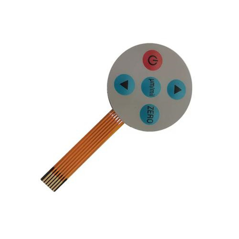
Emerging research hubs, technological parks, and university laboratories in Ostrava leverage our quick-turn frameless foil systems. Sub-millimeter BGA fanouts, rigid-flex circuits, and custom membrane switch panels benefit from our automated DFM aperture optimization routines.
Electronics Manufacturing & SMT Technology Trends in Ostrava
Understanding how Central Europe's evolving high-mix, low-to-medium volume manufacturing landscapes require agile tooling and tighter process windows.
The Shift Toward Step Stencils and Miniaturization (01005 & Ultra-Fine Pitch)
As Czech electronic designers merge high-power converters with dense IoT telemetry on a single board, standard homogeneous stencil foils are often insufficient. Step-down technology creates thinner zones (e.g., thinning a 130µm foil to 100µm) to mitigate paste bridging across fine-pitch ICs, while Step-up technology (chemically etching or micro-welding pockets up to 180µm) provides substantial paste reserves for large connectors and inductors.
Closed-Loop 3D SPI (Solder Paste Inspection) Integration
Assembly plants throughout Ostrava and the wider Moravian-Silesian tech corridor increasingly employ closed-loop 3D SPI platforms (Koh Young, CyberOptics, Mirtec) communicating directly with screen printers. When paste volumetric deviation is detected, automatic stencil offset adjustments and programmable solvent under-wipe cycles are initiated. Our laser stencils maintain micro-fiducials with high contrast, enabling camera systems to lock zero-datum coordinates within 0.1-second cycle times.
Why Global & Regional OEMs Partner with VUKO Electronics
Combining 14+ years of verified international export excellence with end-to-end turnkey hardware integration under one roof.
14+ Years Export Experience
Alibaba.com Onsite-Verified supplier delivering tested, compliant PCBA, FPC, and precision stencils to Tier-1 European clients.
Comprehensive Ecosystem
Fabrication, turnkey PCBA, rigid-flex circuits, aluminum core MCPCBs, and membrane switches with full BOM sourcing support.
Rapid 24h Engineering
Rapid DFM reviews, aperture modifications, and CAM preparation within 24 hours to accelerate development milestones.
Agile Low MOQ Policy
Prototyping stencils and circuit boards starting from 5 pieces, scaling reliably to high-throughput containerized batches.
Frequently Asked Questions for Ostrava SMT Procurement
Clear, definitive technical and commercial answers tailored for engineering teams and supply chain leads.
What CAD/Gerber file formats are required for SMT stencil fabrication?
What frame sizes and frameless systems are compatible with Czech SMT printers?
How do nano-coated stencils benefit ultra-fine pitch printing?
What are the typical lead times and logistics arrangements to Ostrava?
Can you manufacture stepped stencils for mixed-technology boards?
What quality verification steps are executed before dispatch?
Ready to Optimize Your SMT Assembly Yield in Ostrava?
Submit your Gerber files or engineering drawings today. Our seasoned CAM engineers will provide a comprehensive DFM aperture evaluation, foil thickness recommendations, and a direct quotation within 24 hours.
Send an Inquiry